
Display device and method of compensating degradation of a display panel

a technology of display panel and display device, which is applied in the direction of static indicating devices, instruments, etc., can solve the problems of relatively complex (or, complicated) light emitting display device not displaying an image with the intended luminance, and achieve the effect of simple current sensing configuration

Active Publication Date: 2019-06-18
SAMSUNG DISPLAY CO LTD
View PDF11 Cites 1 Cited by
  • Summary
  • Abstract
  • Description
  • Claims
  • Application Information

AI Technical Summary

Benefits of technology

The patent describes a method of compensating for degradation or brightness degradation of a display panel. The method involves sensing the total driving current of the panel and calculating a compensation grayscale for each pixel based on the total driving current and input data provided to the panel. This compensation method can accurately compensate for degradation of the display panel and ensure consistent brightness across the entire panel.

Problems solved by technology

Thus, over time the organic light emitting display device may not display an image with the intended luminance due to degradation of the organic light emitting diode or degradation of the driving transistor.
That is, the related art organic light emitting display device may include a relatively complex (or, complicated) current sensing configuration to sense the current of each of the pixels.

Method used


Image

  • Display device and method of compensating degradation of a display panel
  • Display device and method of compensating degradation of a display panel
  • Display device and method of compensating degradation of a display panel

Examples


Embodiment Construction

[0052]Hereinafter, aspects of example embodiments of the present invention will be explained in more detail with reference to the accompanying drawings, in which like reference numbers refer to like elements throughout. The present invention, however, may be embodied in various different forms, and should not be construed as being limited to only the illustrated embodiments herein. Rather, these embodiments are provided as examples so that this disclosure will be thorough and complete, and will fully convey the aspects and features of the present invention to those skilled in the art. Accordingly, processes, elements, and techniques that are not necessary to those having ordinary skill in the art for a complete understanding of the aspects and features of the present invention may not be described. Unless otherwise noted, like reference numerals denote like elements throughout the attached drawings and the written description, and thus, descriptions thereof will not be repeated. In ...


PUM


Abstract

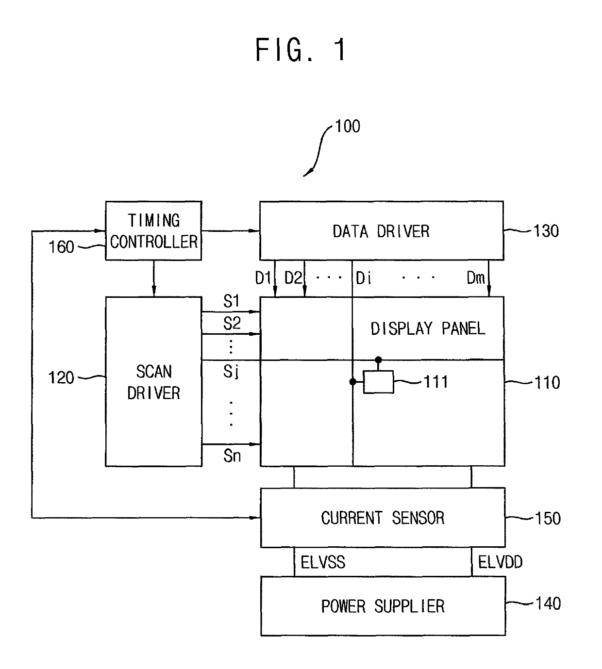
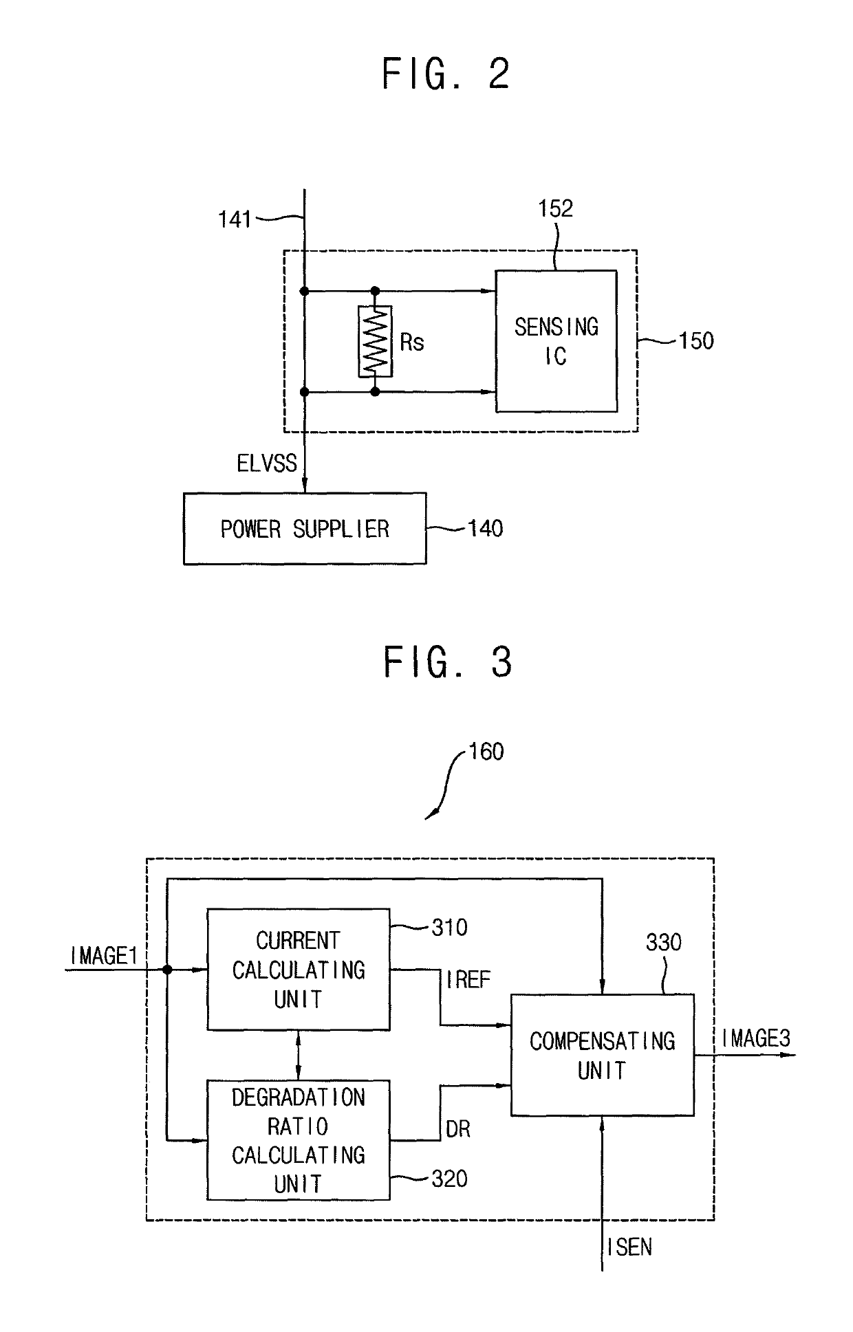
A display device includes a display panel that includes a pixel, a current sensor that measures a driving current provided to the display panel, and a timing controller that calculates a reference driving current and a degradation ratio of the pixel based on first image data provided to the display panel and compensates second image data based on the driving current, the reference driving current, and the degradation ratio of the pixel.

Description

CROSS-REFERENCE TO RELATED APPLICATION(S)[0001]This application claims priority under 35 USC § 119 to Korean Patent Application No. 10-2015-0118259, filed on Aug. 21, 2015 in the Korean Intellectual Property Office (KIPO), the content of which is incorporated herein in its entirety by reference.BACKGROUND[0002]1. Field[0003]Example embodiments of the present invention relate to a display device.[0004]2. Description of the Related Art[0005]An organic light emitting display device displays an image using an organic light emitting diode. The organic light emitting diode and a driving transistor that transfers a current to the organic light emitting diode may degrade over time as the organic light emitting diode and the driving transistor are utilized. Thus, over time the organic light emitting display device may not display an image with the intended luminance due to degradation of the organic light emitting diode or degradation of the driving transistor.[0006]A related art organic lig...

Claims


Application Information

Patent Timeline
Patent Type & Authority Patents(United States)
IPC IPC(8): G09G3/30G09G3/20G09G3/10
CPCG09G3/2092G09G2320/0233G09G2320/0242G09G2320/0271G09G2320/0285G09G2320/0295G09G2320/043G09G2360/16G09G3/006G09G3/3233G09G3/3696G09G3/3208G09G2310/08
Inventor KIM, MIN-CHEOLKIM, IN-HWANJUN, BYUNG-GEUN
Owner SAMSUNG DISPLAY CO LTD
Learn More