Glass product for use in ultra-thin glass display applications

a technology of glass substrate and ultra-thin glass, which is applied in the field of glass substrate products, can solve the problems of increasing the weight of the larger display, affecting the production efficiency of fusion glass thinner,

Inactive Publication Date: 2005-01-06
CORNING INC
View PDF11 Cites 111 Cited by
  • Summary
  • Abstract
  • Description
  • Claims
  • Application Information

AI Technical Summary

Benefits of technology

[0011] The present invention addresses the above-described needs. The present invention provides an ultra-thin fusion glass substrate that can be used in conventional TFT manufacturing processes. The glass substrate product of the present invention has a smoothness that allows the direct formation of thin-film transistors without having to perform a polishing or grinding step. The present invention provides ultra-thin glass substrates having a thickness in the range between 0.4 mm and 0.1 mm. One aspect of the present invention is a s

Problems solved by technology

However, this raises several issues.
First, the increased weight of the larger display is problematic.
Unfortunately, if the thickness of the glass is decreased, the elastic sag of the glass substrate becomes a problem.
Presently, it is difficult for TFT manufacturing technology to accommodate fusion glass thinner that 0.5 mm because of glass sag.
Thinner, larger substrates have a negative impact on the processing robotics' ability to load, retrieve, and s

Method used


Image

  • Glass product for use in ultra-thin glass display applications
  • Glass product for use in ultra-thin glass display applications
  • Glass product for use in ultra-thin glass display applications

Examples


Embodiment Construction

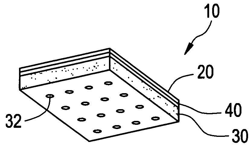
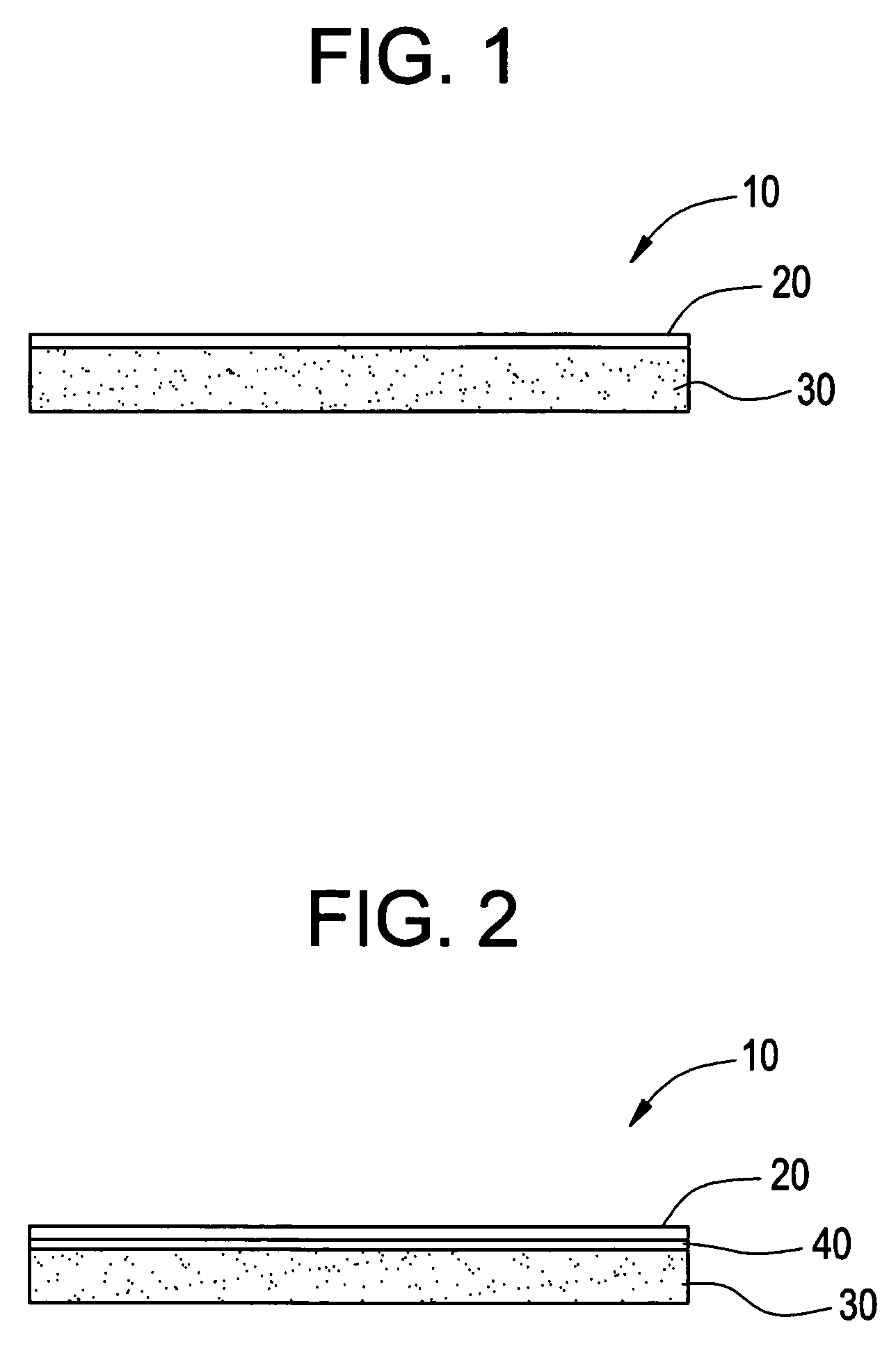
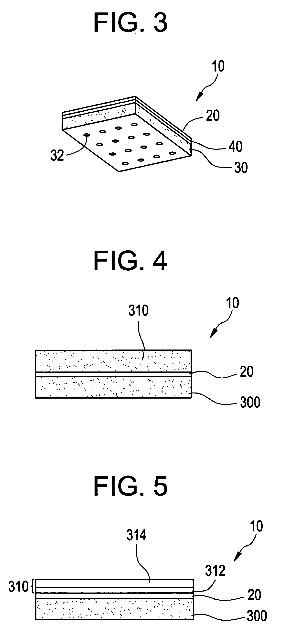
[0024] Reference will now be made in detail to the present exemplary embodiments of the invention, examples of which are illustrated in the accompanying drawings. Wherever possible, the same reference numbers will be used throughout the drawings to refer to the same or like parts. An exemplary embodiment of the substrate product of the present invention is shown in FIG. 1, and is designated generally throughout by reference numeral 10.

[0025] In accordance with the invention, the present invention is directed to a substrate product for use in the manufacture of active matrix liquid crystal display panels. The product includes a display substrate suitable for use as a display panel. The display substrate has a thickness less than or equal to 0.4 mm, a composition that is substantially alkali free, and a surface smoothness that allows the direct formation of thin-film transistors thereon without a prior processing step of polishing and / or grinding. The product also includes at least o...


PUM

PropertyMeasurementUnit
Lengthaaaaaaaaaa
Timeaaaaaaaaaa
Thicknessaaaaaaaaaa

Abstract

The present invention is directed to a substrate product for use in the manufacture of active matrix liquid crystal display panels. The product includes a display substrate suitable for use as a display panel. The display substrate has a thickness less than or equal to 0.4 mm, a composition that is substantially alkali free, and a surface smoothness that allows the direct formation of thin-film transistors thereon without a prior processing step of polishing and/or grinding. The product also includes at least one support substrate removably attached to the display substrate.

Description

BACKGROUND OF THE INVENTION [0001] 1. Field of the Invention [0002] The present invention relates generally to glass substrates, and particularly to a glass substrate product for use in AMLCD display manufacturing processes. [0003] 2. Technical Background [0004] Liquid crystal displays (LCDs) are non-emissive displays that use external light sources. An LCD is a device that may be configured to modulate an incident polarized light beam emitted from the external source. LC material within the LCD modulates light by optically rotating the incident polarized light. The degree of rotation corresponds to the mechanical orientation of individual LC molecules within the LC material. The mechanical orientation of the LC material is readily controlled by the application of an external electric field. This phenomena is readily understood by considering a typical twisted nematic (TN) liquid crystal cell. [0005] A typical TN liquid crystal cell includes two substrates and a layer of liquid crys...

Claims


Application Information

Patent Timeline
IPC IPC(8): B32B7/06B32B17/06B44C1/22C03C19/00C03C27/10C09K19/52G02FG02F1/1333G02F1/136G02F1/1362
CPCB32B7/06B32B17/06C03C19/00C03C27/10Y10T428/10G02F1/1333G02F2001/133302G02F2001/13613G02F2001/136295C03C2218/355C09K2323/00G02F1/133302G02F1/13613G02F1/136295B32B3/266B32B3/28B32B7/12B32B2038/0064B32B2309/105B32B2457/202
Inventor BOCKO, PETER L.COPPOLA, FRANK T.EDWARDS, VICTORIA A.GILLBERG, GUNILLA E.LAPP, JOSEF C.MASHEWSKE, MONICA J.SCHAEFFLER, ROBERT G.TAMMARO, DAVID A.
Owner CORNING INC
Why Eureka
Try Eureka