High aperture ratio in-plane switching mode active matrix liquid crystal display unit

a liquid crystal display unit and in-plane switching technology, applied in non-linear optics, instruments, optics, etc., can solve the problems of unsatisfactory aperture ratio of prior art lcd units, data lines still are not satisfactorily shielded from liquid crystal layers, and the backlight that passes through the edges of data lines to leak to the viewer side. to achieve the effect of high aperture ratio

Active Publication Date: 2007-11-29
HANNSTAR DISPLAY CORPORATION
View PDF6 Cites 47 Cited by
  • Summary
  • Abstract
  • Description
  • Claims
  • Application Information

AI Technical Summary

Benefits of technology

[0007]It is therefore an object of the present invention to provide an in-plane sw

Problems solved by technology

However, the data lines are not shielded from the liquid crystal layer, the electric fields of the data lines adversely affect the orientation of the liquid crystals and cause portions of the backlight that pass through the edges of the data line to leak to the viewer side.
Since the black matrix occupies a relatively large space, the aperture ratio of the prior art LCD unit is not satisfactory.
Although the data lines of Document 2 are covered with the outer edge portions of the common electrodes, the data lines are still not satisfactorily shielded from the liquid crystal layer.
T

Method used


Image

  • High aperture ratio in-plane switching mode active matrix liquid crystal display unit
  • High aperture ratio in-plane switching mode active matrix liquid crystal display unit
  • High aperture ratio in-plane switching mode active matrix liquid crystal display unit

Examples


Embodiment Construction

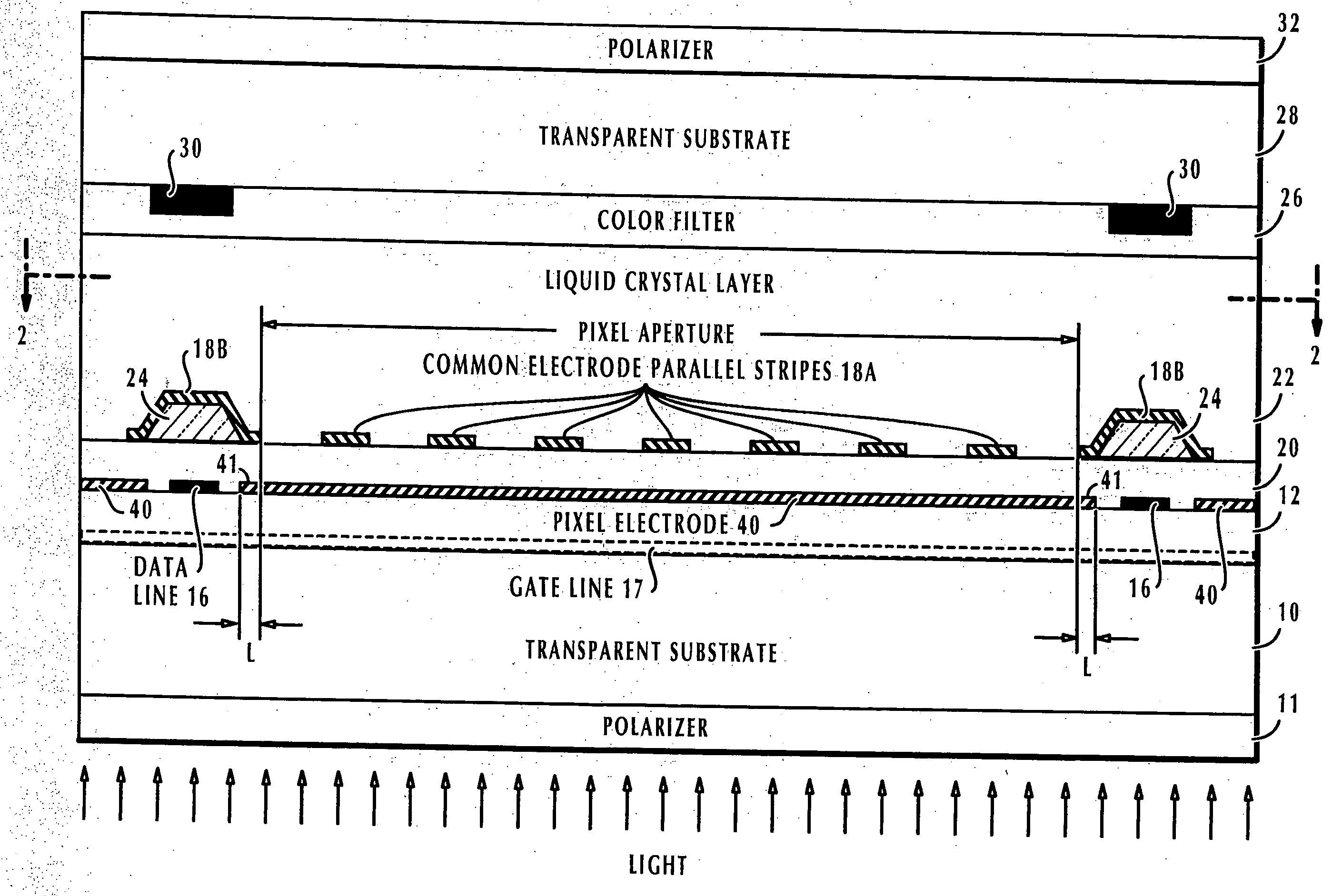
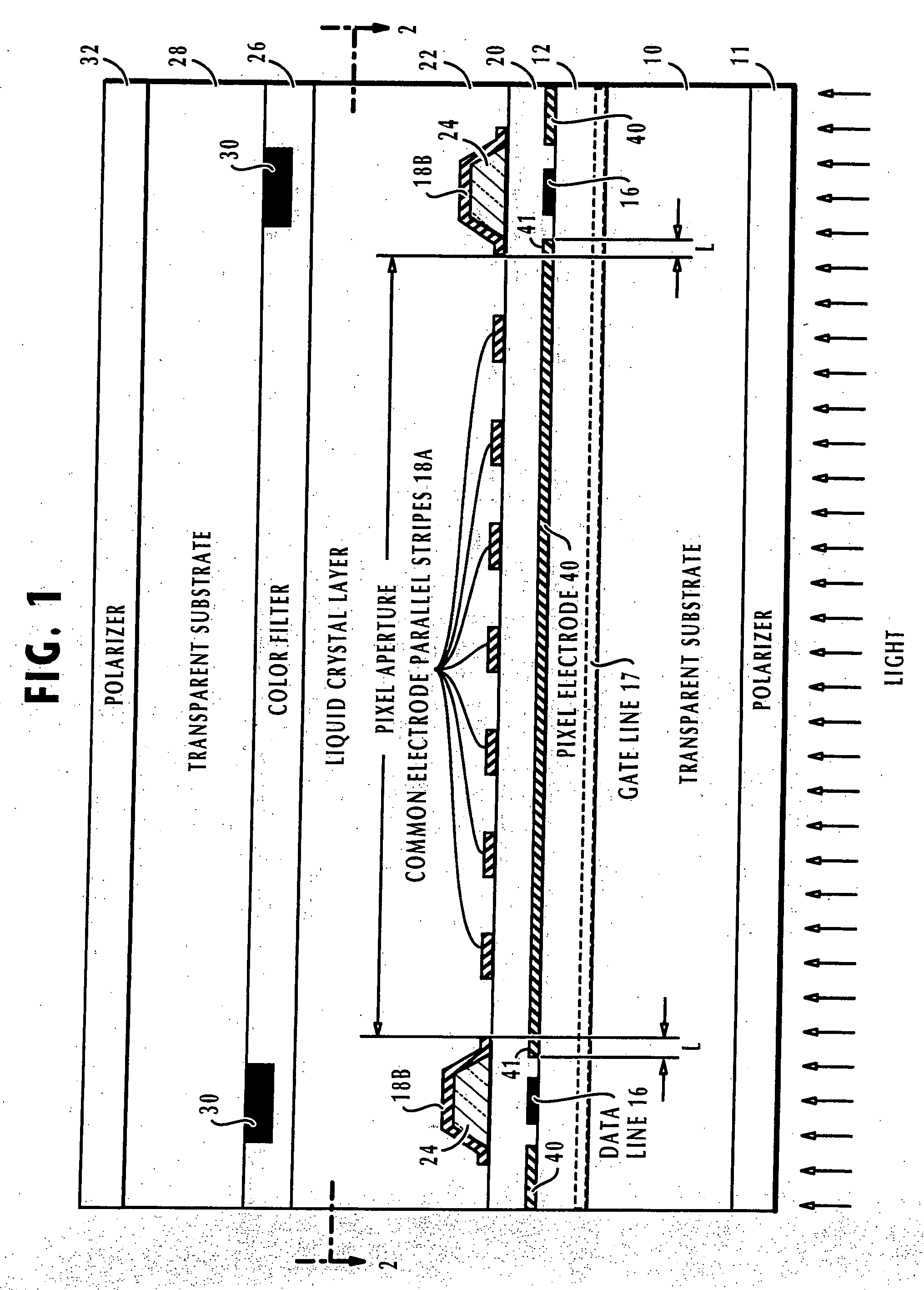
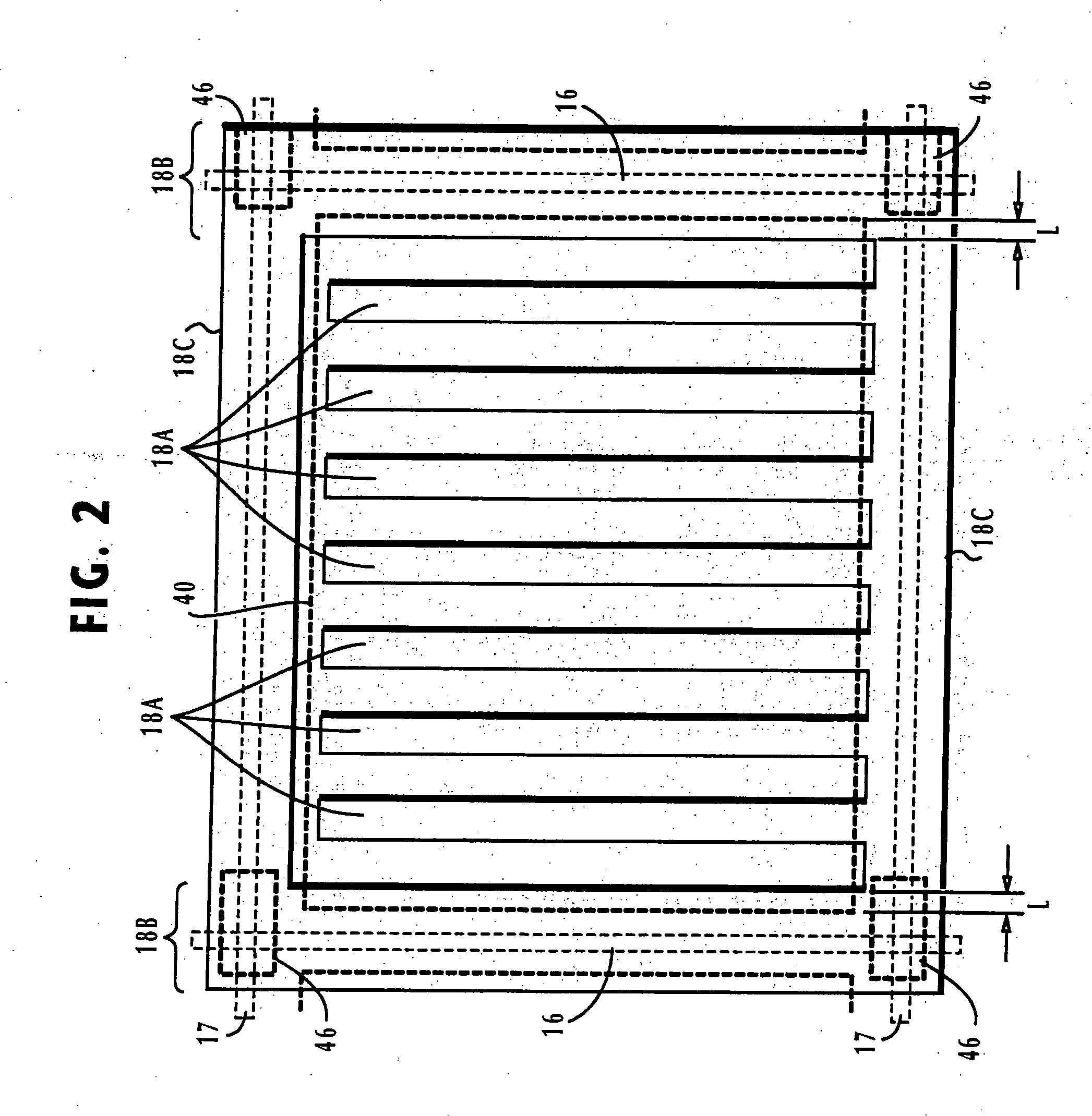
[0017]FIG. 1 shows, in vertical cross-section, an in-plane switching mode active matrix liquid crystal display unit according to a first embodiment of the present invention. The LCD unit comprises a transparent substrate 10 on a polarizer 11, which is exposed to backlight. On the substrate 10 a plurality of parallel gate lines 17 are formed, the gate lines 17 being covered with a transparent insulating layer 12. On the insulating layer 12 are a pattern of parallel data lines 16 extending crosswise to the gate lines 17 to define a matrix pattern of pixels with the data lines 16. A pattern of pixel electrodes 40 are formed on the insulating layer 12 so that each pixel electrode 40 is positioned at an intersection of a data line 16 and a gate line 17. The data lines 16 and the pixel electrodes 40 are covered with a transparent insulating layer 20 for protecting thin-film transistors not shown. On the insulating layer 20, a pattern of insulators 24 is formed with polymer so that each in...


PUM


Abstract

In a liquid crystal display unit where a matrix pattern of pixels are defined by gate lines and crosswise data lines, transparent pixel electrodes are formed on the same layer as the data lines and corresponding transparent common electrodes are formed above the transparent pixel electrodes. On the common electrodes the liquid crystal layer is provided. In the aperture of each pixel, the common electrode has a pattern of parallel stripe portions and a peripheral portion outside of the aperture for shielding the field of the corresponding data line. Each pixel electrode cooperates with that parallel stripe portions of the corresponding common electrode to produce inner fringe fields along such parallel stripe portions and has portions that overlap the peripheral portions of the common electrode to produce peripheral fringe fields so that liquid-crystal cells can be uniformly in-plane switched by the inner fringe fields as well as by the peripheral fringe fields.

Description

BACKGROUND OF THE INVENTION[0001]1. Field of the Invention[0002]The present invention relates to an in-plane switching (IPS) mode active matrix liquid crystal display unit.[0003]2. Description of the Related Art[0004]Japanese Patent Publication 2005-70747 (referred to as Document 1) discloses a liquid crystal display unit, which can be classified into one of IPS-mode display units. The prior art display unit comprises a lower structure and an upper structure and accommodates a liquid crystal layer between the upper and lower structures. The whole unit is illuminated with backlight provided below the lower structure. The lower structure consists of a transparent substrate on which a transparent common electrode (first ITO electrode) is formed and coated with an insulating layer. For each pixel, a data line is provided on the insulating layer and coated with a protection layer, on which transparent parallel pixel electrodes (second ITO electrodes) are provided. However, the data lines...

Claims


Application Information

Patent Timeline
IPC IPC(8): G02F1/1343
CPCG02F1/134363G02F2201/40G02F2001/134372G02F1/134372
Inventor KAWASAKI, TAKUKONNO, TAKAYUKINISHIDA, SHINICHI
Owner HANNSTAR DISPLAY CORPORATION
Why Eureka
Try Eureka