Semiconductor device and method of manufacturing thereof

a semiconductor and capacitor technology, applied in the field of semiconductor devices, can solve the problems of reducing layout efficiency, difficult to make a large storage capacitor and a high aperture ratio compatible with each other, and strict demand for capacitor wiring resistance, so as to achieve high aperture ratio, reduce load, and high display quality

Inactive Publication Date: 2006-08-29
SEMICON ENERGY LAB CO LTD
View PDF24 Cites 68 Cited by
  • Summary
  • Abstract
  • Description
  • Claims
  • Application Information

AI Technical Summary

Benefits of technology

[0024]The present invention has been made in view of the above problems as a solution for the designing side, and therefore has an object to provide a liquid crystal display device having high quality display by obtaining a high aperture ratio while securing a sufficient storage capacitor (Cs), and at the same time, by dispersing a load (a pixel writing-in electric current) of the capacitor wiring in a timely manner to effectively reduce the load.

Problems solved by technology

Such demands become problems in proceeding with the progress of making the pitch of each display pixel microscopic which accompanies the progress of making a liquid crystal display device smaller and high definition (increasing the number of pixels).
There is an additional problem in that it is difficult to make a high aperture ratio and a large storage capacitor compatible with each other in the above stated conventional pixel structure.
The gate insulating film of the A region is not rendered its original function, becoming a cause of reducing the efficiency of layout.
Further, in the case of the above structure, there is a problem in that the demand for a capacitor wiring resistance has become strict.

Method used


Image

  • Semiconductor device and method of manufacturing thereof
  • Semiconductor device and method of manufacturing thereof
  • Semiconductor device and method of manufacturing thereof

Examples


embodiment 1

[Embodiment 1]

[0096]Hereinafter, embodiments of the present invention will be described taking a point sequential drive of a projector type liquid crystal display device as an example.

[0097]An active matrix type liquid crystal display device utilizing a TFT as its switching element is constructed of a substrate (TFT substrate) with pixel electrodes arranged in matrix and an opposing substrate with opposing electrodes formed thereon arranged facing the TFT substrate via a liquid crystal layer. The space between the two substrates are controlled at a predetermined interval via spacers, etc. and a sealing material is used around the outer periphery portion of the display region to enclose the liquid crystal layer.

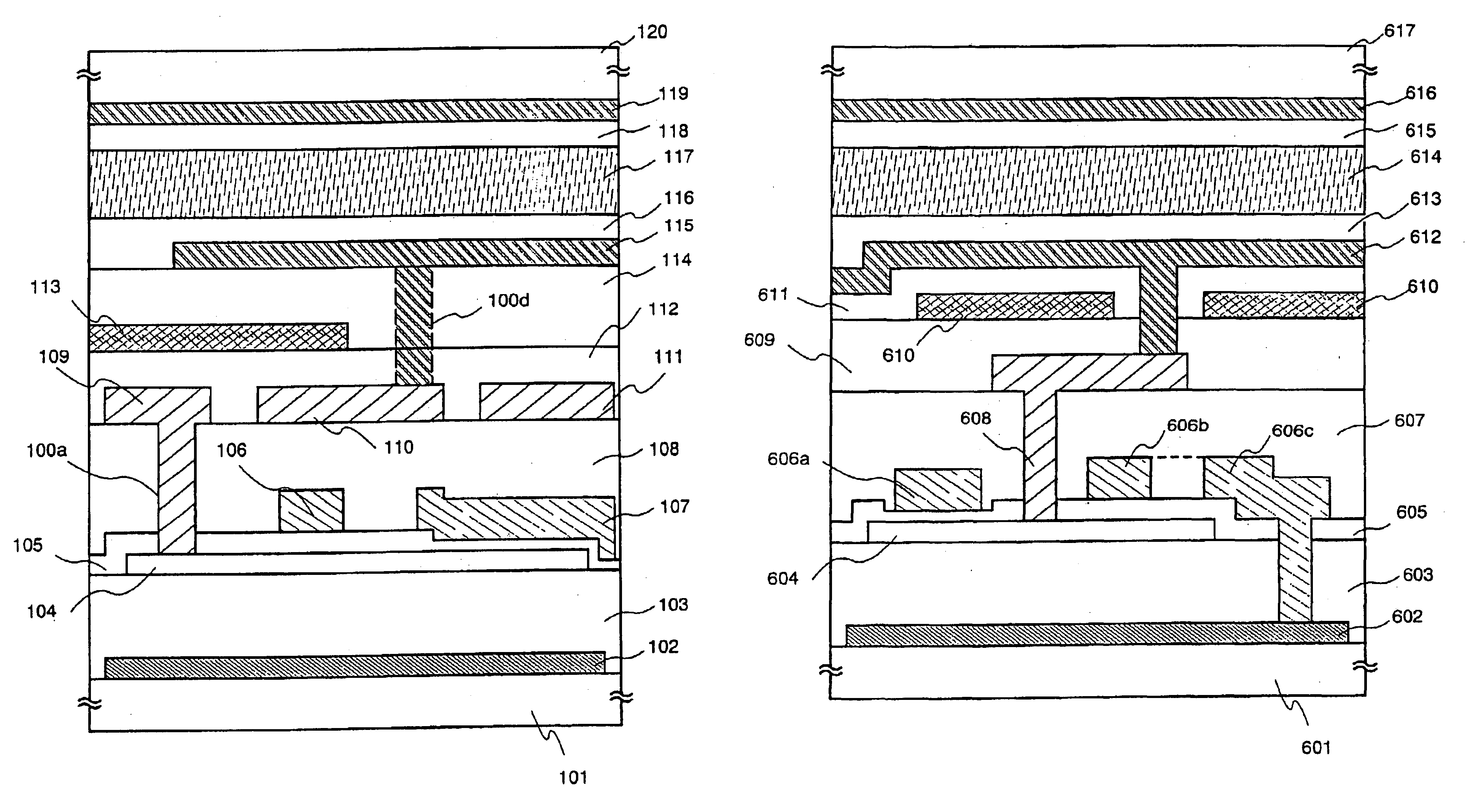
[0098]FIG. 4 is a view schematically showing a cross-sectional structure of the liquid crystal display device of the present embodiment. In FIG. 4, reference numeral 101 denotes a substrate (TFT substrate), 102 denotes the scanning lines, 103 denotes a first insulating film, 1...

embodiment 2

[Embodiment 2]

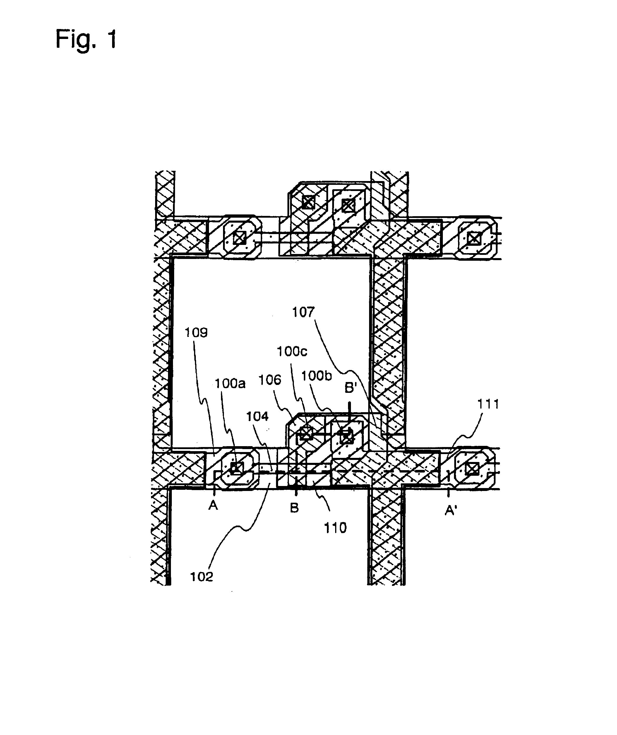
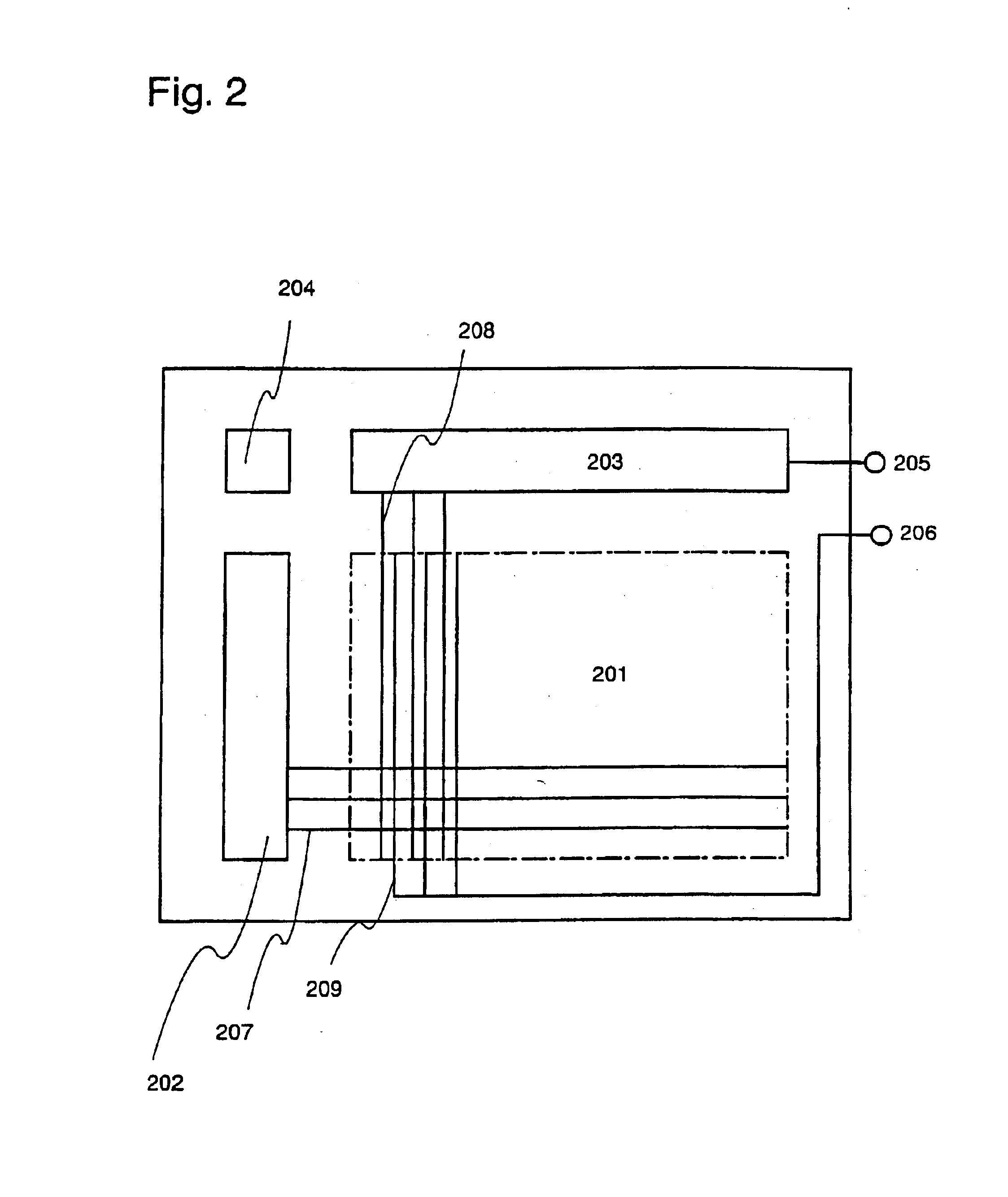
[0134]A structure of the active matrix type liquid crystal display device shown in Embodiment 1 will be described here in Embodiment 2 with reference to the perspective view of FIG. 5. It is to be noted that the same reference numerals designate components corresponding to those in Embodiment 1.

[0135]In FIG. 5, a matrix substrate is composed of a pixel portion, a scanning line driver circuit 802, a signal line driver circuit 803, and other signal processing circuits formed on a substrate 101. A pixel TFT 800 and a storage capacitor 200 are provided in the pixel portion, and the driver circuits provided in the periphery thereof are structured based on a CMOS circuit.

[0136]Further, the capacitor wiring 107 is provided in a direction parallel with the signal line 109 and functions as the upper electrode of the storage capacitor 200. The capacitor wiring 107 is also connected to the ground or to a fixed electric potential.

[0137]The scanning line 102 and the signal line 109...

embodiment 3

[Embodiment 3]

[0138]The pixel matrix circuit formed by implementing the present invention can be used in various electro-optical devices (active matrix type liquid crystal display device, active matrix EL display, and active matrix EC display). That is, the present invention can be implemented in all electronic equipment that incorporate these electro-optical devices as a display portion.

[0139]The following can be given as such electronic equipment: a video camera, a digital camera, a projector (a rear type or a front type), a head mount display (goggle type display), a car navigation system, a personal computer, a portable information terminal (such as a mobile computer, a cellular phone, and an electronic book) etc. Some examples of these are shown in FIGS. 6A to 6F and FIGS. 7A to 7D.

[0140]FIG. 6A shows a personal computer that is comprised of a main body 2001, an image input portion 2002, a display portion 2003, and a keyboard 2004. The present invention can be applied to the di...


PUM

PropertyMeasurementUnit
thicknessaaaaaaaaaa
sizeaaaaaaaaaa
areasaaaaaaaaaa

Abstract

To provide a liquid crystal display device having high quality display by obtaining a high aperture ratio while securing a sufficient storage capacitor (Cs), and at the same time, by dispersing a load (a pixel writing-in electric current) of a capacitor wiring in a timely manner to effectively reduce the load. A scanning line is formed on a different layer from a gate electrode and the capacitor wiring is arranged so as to be parallel with a signal line. Each pixel is connected to the individually independent capacitor wiring via a dielectric. Therefore, variations in the electric potential of the capacitor wiring caused by a writing-in electric current of a neighboring pixel can be avoided, whereby obtaining satisfactory display images.

Description

BACKGROUND OF THE INVENTION[0001]1. Field of the Invention[0002]The present invention relates to a semiconductor device having a circuit constructed of a thin film transistor (hereinafter referred to as TFTs) and a method of manufacturing the same. For example, the present invention relates to an electro-optical device typified by a liquid crystal display panel, and electronic equipment having such an electro-optical device mounted thereon as a part.[0003]It is to be noted that a semiconductor device as used herein throughout the present specification denotes a general device which functions by utilizing semiconductor characteristics, and that electro-optical devices, semiconductor circuits, and electronic equipments are all semiconductor devices.[0004]2. Description of the Related Art[0005]Techniques for structuring a thin film transistor (TFT) using a semiconductor thin film (having a thickness on the order of about several to several hundred nm) formed on a substrate having an in...

Claims


Application Information

Patent Timeline
Patent Type & Authority Patents(United States)
IPC IPC(8): H01L21/00G02F1/1343G02F1/1345G02F1/136G02F1/1362G02F1/1368G09F9/30G09G3/36H01L21/3205H01L21/768H01L21/77H01L21/822H01L21/84H01L23/52H01L23/522H01L27/04H01L27/12H01L29/786H04N5/66
CPCG02F1/13454H01L27/1214G02F1/136213G02F1/136227G02F1/136286H01L27/3265H01L27/3276H01L29/78633H01L27/1255H01L29/786G02F1/136277G02F1/133345G02F1/1368H01L27/12G02F1/136209H10K59/1216H10K59/131H10K59/12H10K59/123H10K59/1213H01L27/124H01L29/4908
Inventor SHIBATA, HIROSHIISOBE, ATSUO
Owner SEMICON ENERGY LAB CO LTD
Why Eureka
Try Eureka