Pixel drive circuit of OLED (Organic Light Emitting Diode) display and drive method thereof

A pixel driving circuit and driving method technology, applied in static indicators, instruments, etc., can solve the problems affecting the use of large-screen high-resolution displays, and the long charging time of current-programmed pixel driving circuits, so as to improve the aperture ratio and circuit Simple and reliable, the effect of prolonging the service life

Inactive Publication Date: 2011-02-16
SOUTH CHINA UNIV OF TECH
View PDF5 Cites 65 Cited by
  • Summary
  • Abstract
  • Description
  • Claims
  • Application Information

AI Technical Summary

Problems solved by technology

Generally speaking, the current-programmed pixel driving circuit needs a long charging time when displaying low grayscale, which affects its use in large-screen high-resolution displays.

Method used


Image

  • Pixel drive circuit of OLED (Organic Light Emitting Diode) display and drive method thereof
  • Pixel drive circuit of OLED (Organic Light Emitting Diode) display and drive method thereof
  • Pixel drive circuit of OLED (Organic Light Emitting Diode) display and drive method thereof

Examples


Embodiment

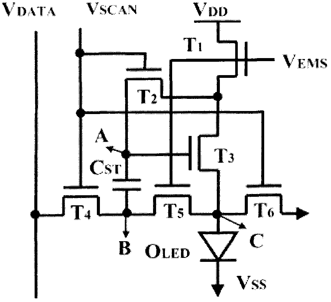
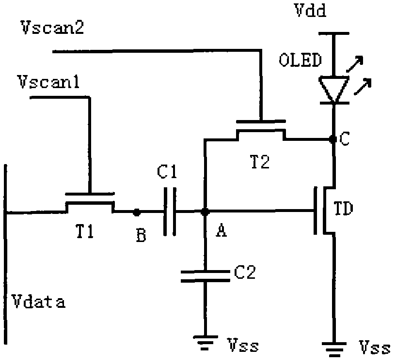
[0029] Such as image 3 As shown, the pixel driving circuit of the OLED display of the present invention includes a first switching transistor T1, a second switching transistor T2, a driving transistor TD, and an OLED light emitting diode. The drain of the first switching transistor T1 is connected to the data line Vdata, the gate is connected to the first scanning control line Vscan1, and the source is connected to the B terminal of the coupling capacitor C1. The first switching transistor T1 controls the coupling capacitor C1 to write to the gate of the drive transistor. Enter the grayscale data voltage.

[0030] The drain of the second switching transistor T2 is connected to the A terminal of the storage capacitor C2 and the coupling capacitor C1, the gate is connected to the second scanning control line Vscan2, the source is connected to the drain of the driving transistor TD, and is connected to the power line Vdd through the organic light emitting diode. connected, the ...


PUM


Abstract

The invention discloses a pixel drive circuit of an OLED (Organic Light Emitting Diode) display and a drive method thereof. The pixel circuit comprises a drive transistor, two switching transistors, a coupling capacitor, a storage capacitor and an OLED, wherein the drain electrode of the first switching transistor is connected with a data line, the grid electrode is connected with a first scanning control line, and the source electrode is connected with the end B of the coupling capacitor; the drain electrode of the second switching transistor is connected with the storage capacitor and the end A of the coupling capacitor, the grid electrode is connected with a second scanning control line, and the source electrode is connected with the drain electrode of the drive transistor and is connected with a power line through the OLED; and the grid electrode of the drive transistor is connected with the storage capacitor and the end A of the coupling capacitor, and the source electrode is grounded. The circuit can be used for effectively compensating the heterogeneity of threshold voltage of a thin film transistor and the degeneration of the cut-in voltage of the OLED to improve the picture brightness homogeneity of the OLED display screen.

Description

technical field [0001] The invention relates to a pixel driving technology of a light emitting diode display, in particular to a pixel driving circuit of a light emitting diode display and a driving method thereof. Background technique [0002] With the development of display technology, passive array OLED has been unable to meet the requirements of high resolution and large amount of information display. For large-screen high-resolution displays, active array drive methods are usually used. [0003] Currently, thin film transistors used in active array OLEDs mainly include hydrogenated amorphous silicon thin film transistors (a-Si:H TFT) and low temperature polysilicon thin film transistors (LTPS TFT). The threshold voltage of a-Si:H TFT will drift with the working time. To solve this problem, Jae-Hoon Lee et al. :H TFT and OLED for Active Matrix OLED" (IEEE ELECTRON DEVICE LETTERS, VOL.26, NO.12, DECEMBER 2005) once proposed a compensation circuit, the pixel drive circui...

Claims


Application Information

Patent Timeline
Patent Type & Authority Applications(China)
IPC IPC(8): G09G3/32G09G3/3225
Inventor 吴为敬周雷颜骏许志平赖志成
Owner SOUTH CHINA UNIV OF TECH
Why Eureka
Try Eureka