Semiconductor device and method for manufacturing the same

a semiconductor and transistor technology, applied in semiconductor devices, optics, instruments, etc., can solve problems such as conductive films, current leakage between pixel electrodes, and easy generation of residues, and achieve the effects of reducing contact resistance, reducing leakage current or conductivity due to residues, and high light transmission

Active Publication Date: 2007-06-28
SEMICON ENERGY LAB CO LTD
View PDF28 Cites 67 Cited by
  • Summary
  • Abstract
  • Description
  • Claims
  • Application Information

AI Technical Summary

Benefits of technology

[0090]In the same way, a residue generated when etching a transparent conductive material during formation of a pixel electrode can be reduced and leakage current or conductivity due to the residue can be reduced.
[0091]By the present invention, disclination of liquid crystals in the vicinity of the portion over a contact hole due to a shape of the contact hole of a protective film, which has been conventionally generated, can be eliminated.
[0092]Furthermore, by the present invention, by increasing an area where a pixel electrode and a drain electrode are in contact with each other, contact resistance can be reduced.
[0093]A high transmission of light from a light source in the opening of the protective film can be obtained.
[0094]In the present invention, the number of photomasks is not required to be increased in comparison with conventional liquid crystal display devices, and a high-quality liquid crystal display device can be manufactured without increasing the number of manufacturing steps and manufacturing costs.
[0095]As described above, by the present invention, a liquid crystal display device with high reliability, high yield, high luminance, and high aperture ratio can be provided.

Problems solved by technology

However, the transparent conductive film exemplified above is disadvantageous in that a residue is easily generated in comparison with metal such as aluminum (Al).
Therefore, when a residue is generated and remains over a substrate eventually, current leak might be caused between pixel electrodes.
As is the case with the above transparent conductive film, an insulating film such as a silicon nitride film or a silicon oxide film is disadvantageous in that a residue generated due to wet etching remains in a connection portion between conductive materials.
Therefore, there is concern that contact defect or increase in contact resistance might be caused.
Moreover, a wavelength of the light is changed from that of the light source after penetrating the protective film for the same reason, and a difference between a color displayed practically and an intended color may be caused.
However, in the second method, there are problems in that an opening ratio is decreased because an area for forming the electrode is necessary in order to provide the auxiliary capacitor line as one of the electrodes in addition to the scanning line (the gate wiring) and yield is decreased because the electrode formed of the same material and formed in the same layer as those of the drain electrode is formed as the other electrode.
For this reason, problems in that the scanning line itself has to be wide and a portion of the scanning line overlapping with the pixel electrode has to be taken large in design occur.
However, a concave is caused on an alignment film due to the contact hole under the alignment film; therefore, ideal rubbing is difficult.
For this reason, there is a disadvantage in that disclination of liquid crystals arranged near the portion over the contact hole occurs.
Therefore, there is a problem in that quality of display could be poor because light leaks near the portion over the contact hole.
However, this method is one of factors that decrease an aperture ratio.
Eventually, the residue can seriously damage a function as a liquid crystal display device or make the liquid crystal display impossible to work out.
However, although, in a structure of the conventional liquid crystal display device, a circular contact hole with a small diameter is used in a contact portion between the pixel electrode and the drain electrode, it has been concerned that a residue or a cleaning liquid might remain on the inner wall or at the bottom of the circular contact hole when a substrate with a surface to be processed is drawn from cleaner after cleaning.
In addition, it has been concerned that, with such a conventional contact hole with a small diameter, the pixel electrode and the drain electrode could be disconnected due to a bump and poor connection might occur.

Method used


Image

  • Semiconductor device and method for manufacturing the same
  • Semiconductor device and method for manufacturing the same
  • Semiconductor device and method for manufacturing the same

Examples


embodiment 1

[0225]In this embodiment, an example of forming an island-shaped semiconductor film by etching a semiconductor film with the use of a resist mask which is used for forming a source electrode and source wiring and a drain electrode will be explained with reference to FIGS. 14A to 14D, FIGS. 15A and 15B, and FIGS. 18A and 18B. It is to be noted that a portion which is not explained follows the description of Embodiment Mode.

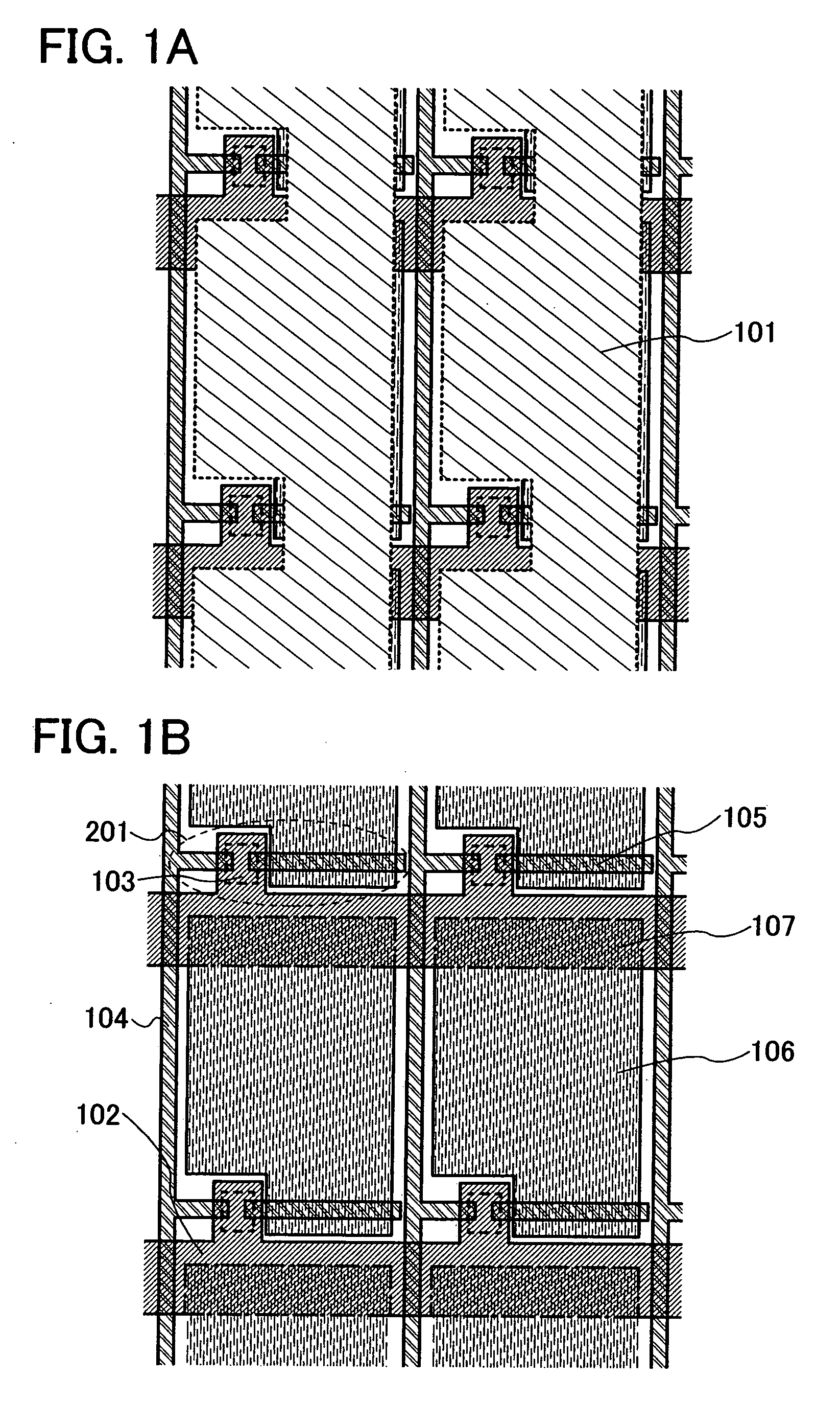
[0226]First, a gate electrode and gate wiring 302 is formed over a substrate 300 (see FIG. 14A). The same substrate as the substrate 100 in Embodiment Mode may be used for the substrate 300. In addition, the gate electrode and gate wiring 302 may be formed of the same material and formed by the same manufacturing process as those of the gate electrode and gate wiring 102 in Embodiment Mode.

[0227]Then, a gate insulating film 308, an amorphous semiconductor film 321, a semiconductor film 322 containing an impurity imparting one conductivity type, and a conductive fil...

embodiment 2

[0247]In this embodiment, a different example from that of Embodiment 1, in a method for forming an island-shaped semiconductor film by etching a semiconductor film with the use of a resist mask used when forming a source electrode and source wiring and a drain electrode, will be explained with reference to FIGS. 16A to 16D, FIGS. 17A to 17D, and FIGS. 19A and 19B. It is to be noted that a portion which is not expressly explained follows the description of Embodiment Mode and Embodiment 1.

[0248]First, by the same process as that of Embodiment Mode or Embodiment 1, a gate electrode and gate wiring 332 is formed over a substrate 330 (see FIG. 16A), and a gate insulating film 338, an amorphous semiconductor film 341, and a semiconductor film 342 containing an impurity imparting one conductivity type are formed thereover (see FIG. 16B).

[0249]Next, a photolithography process is performed, a resist mask is formed, the amorphous semiconductor film 341 and the semiconductor film 342 contain...

embodiment 3

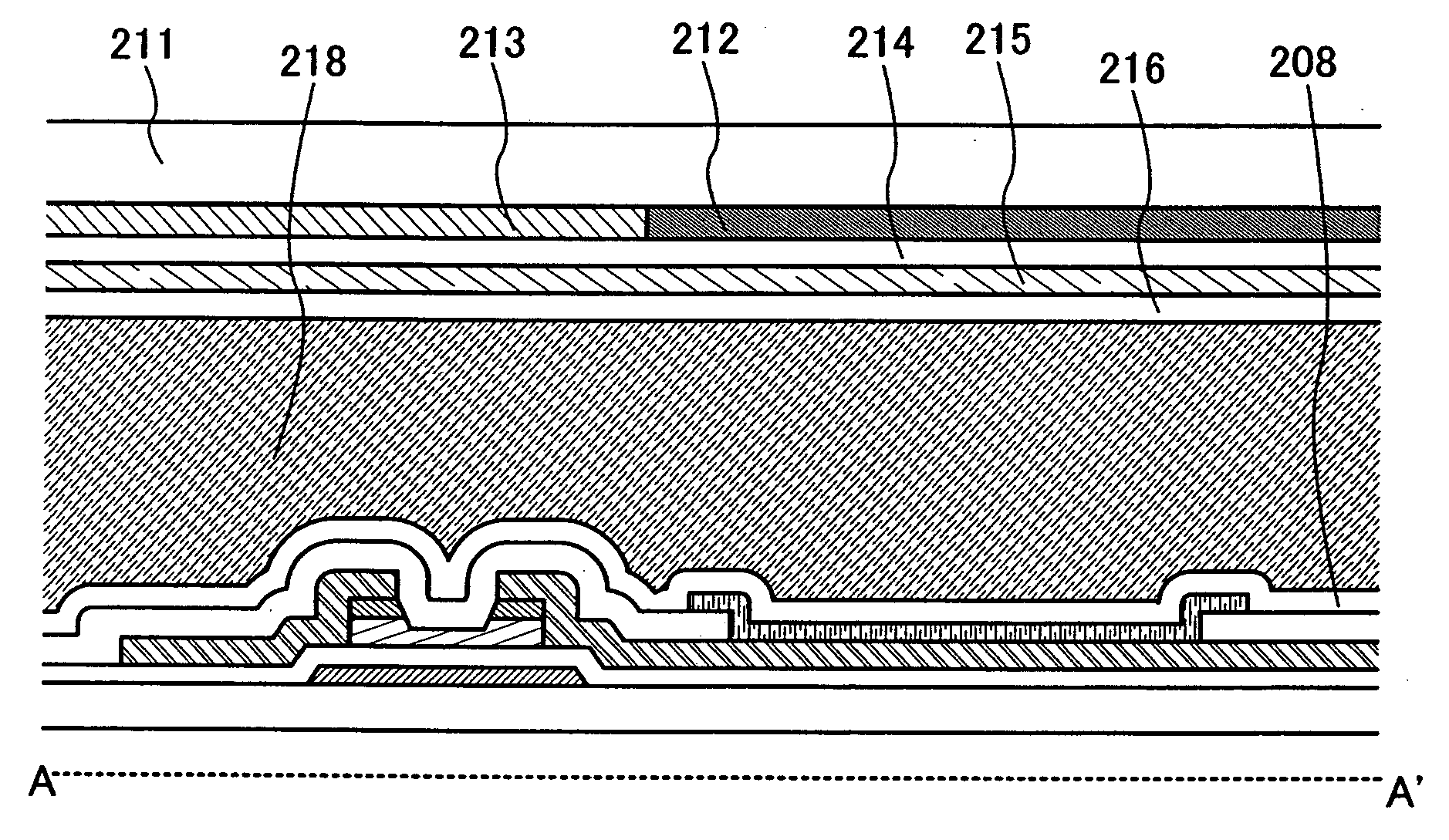
[0259]In this embodiment, an example of preventing a drain electrode from being damaged when a protective film is formed by etching an insulating film formed from a protective film material by forming the drain electrode as a stacked film will be explained with reference to FIGS. 20A to 20E and FIGS. 21A to 21E.

[0260]In Embodiment Mode, an insulating film formed from a protective film material is etched by dry etching by a fourth photolithography process. A drain electrode 105 formed under the insulating film can be terribly damaged when the drain electrode 105 is exposed, depending on a manufacturing condition such as a kind of etching gas, reaction pressure, a substrate temperature, or high frequency.

[0261]If the drain electrode 105 is damaged, electrical connection between the drain electrode 105 and a pixel electrode 106 may be adversely affected.

[0262]Therefore, in this embodiment, by forming a drain electrode of a stacked film including a plurality of layers, the drain electro...


PUM

PropertyMeasurementUnit
thicknessaaaaaaaaaa
thicknessaaaaaaaaaa
thicknessaaaaaaaaaa

Abstract

It is an object to obtain a liquid crystal display device in which a contact defect is reduced, increase in contact resistance is suppressed, and an opening ratio is high. The present invention relates to a liquid crystal display device having a substrate; a thin film transistor provided over the substrate, which includes a gate wiring, a gate insulating film, an island-shaped semiconductor film, a source region, and a drain region; a source wiring which is provided over the substrate and is connected to the source region; a drain electrode which is provided over the substrate and is connected to the drain region; an auxiliary capacitor provided over the substrate; a pixel electrode connected to the drain electrode; and a protective film formed so as to cover the thin film transistor and the source wiring, where the protective film has an opening, and the auxiliary capacitor is formed in the area where the opening is formed.

Description

BACKGROUND OF THE INVENTION[0001]1. Field of the Invention[0002]The present invention relates to a bottom gate thin film transistor (hereinafter, abbreviated as a TFT) in which an amorphous semiconductor film provided over a substrate is used, a circuit formed by the TFT, a device including the circuit formed by the TFT, and a manufacturing method thereof.[0003]In particular, the present invention relates to an electrooptic device typified by a liquid crystal display device and a technique which can be favorably applied to an electronic appliance provided with such an electrooptic device.[0004]2. Description of the Related Art[0005]In recent years, a direct-view liquid crystal display device is widely used in order to display an image or character information on an electronic appliance such as a monitor of a laptop personal computer or a desktop personal computer, a mobile phone, an audio reproducing device, a television device, a mobile terminal, a digital still camera, a video cam...

Claims


Application Information

Patent Timeline
Patent Type & Authority Applications(United States)
IPC IPC(8): G02F1/136
CPCG02F1/1362G02F2201/50G02F1/1368G02F1/136227H01L27/124H01L27/1255
Inventor HOSOYA, KUNIO
Owner SEMICON ENERGY LAB CO LTD
Why Eureka
Try Eureka