Image conversion device, image conversion method and data conversion circuit as well as digital camera

Inactive Publication Date: 2006-01-12
MEGACHIPS
View PDF10 Cites 23 Cited by
  • Summary
  • Abstract
  • Description
  • Claims
  • Application Information

AI Technical Summary

Benefits of technology

[0083] In accordance with the fortieth aspect, it is possible to reduce color breaking phenomenon, and to output color field sequential data with high quality so as to display motion images.
[0084] In accordance with the forty-first aspect, it is possible to greatly reduce the positional offset phenomenon, and consequently to output interpolated data with high quality so as

Problems solved by technology

Since EVF514 acquires respective color fields in time series, it is susceptible to a problem, so-called “color breaking” phenomenon, in which a moving subject tends to be displayed at different positions in respective color fields.
However, when the frame rate conversion is carried out using a buffer memory having a capacity of one frame, as shown in FIG. 49, a problem arises in whi

Method used


Image

  • Image conversion device, image conversion method and data conversion circuit as well as digital camera
  • Image conversion device, image conversion method and data conversion circuit as well as digital camera
  • Image conversion device, image conversion method and data conversion circuit as well as digital camera

Examples


first preferred embodiment

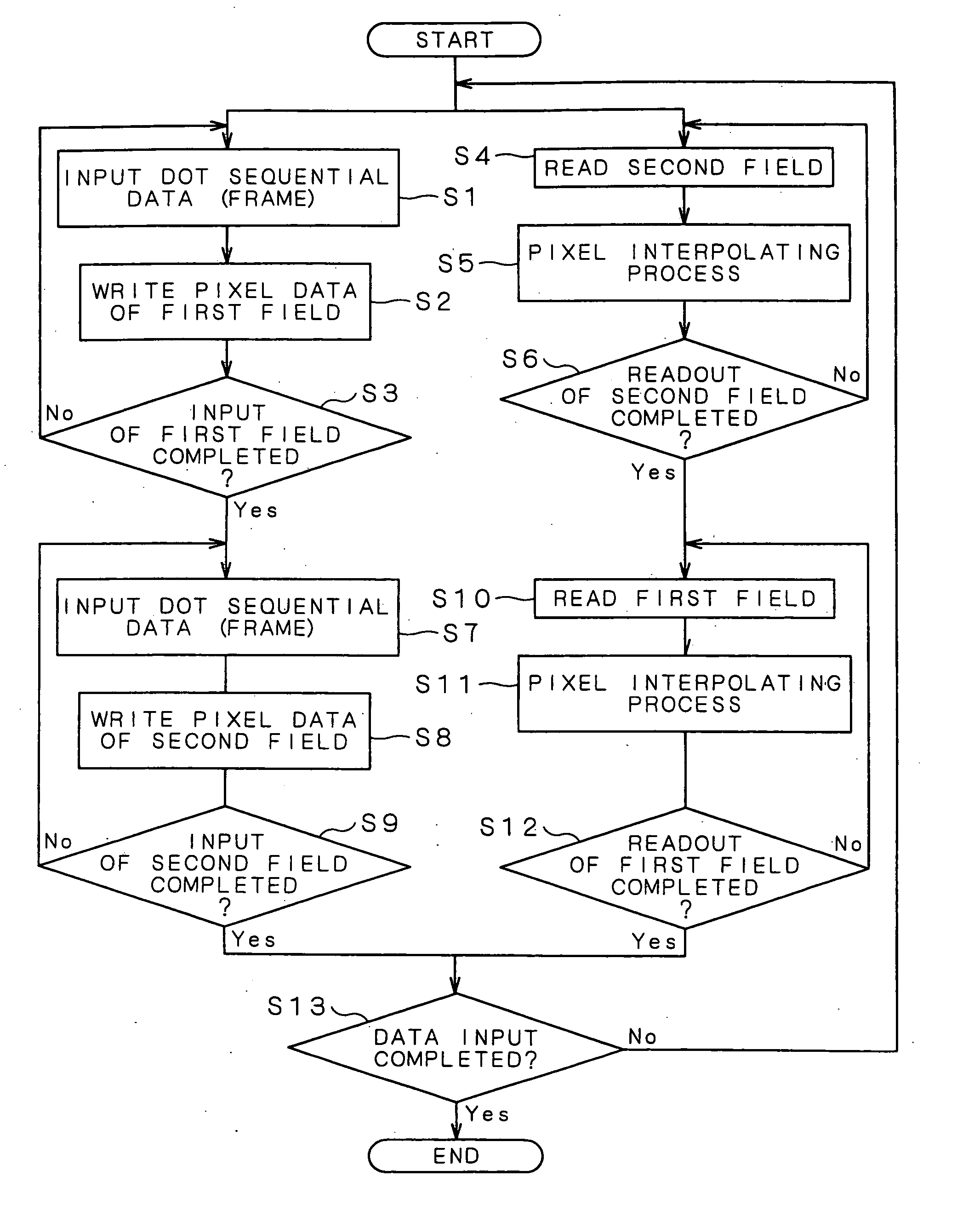
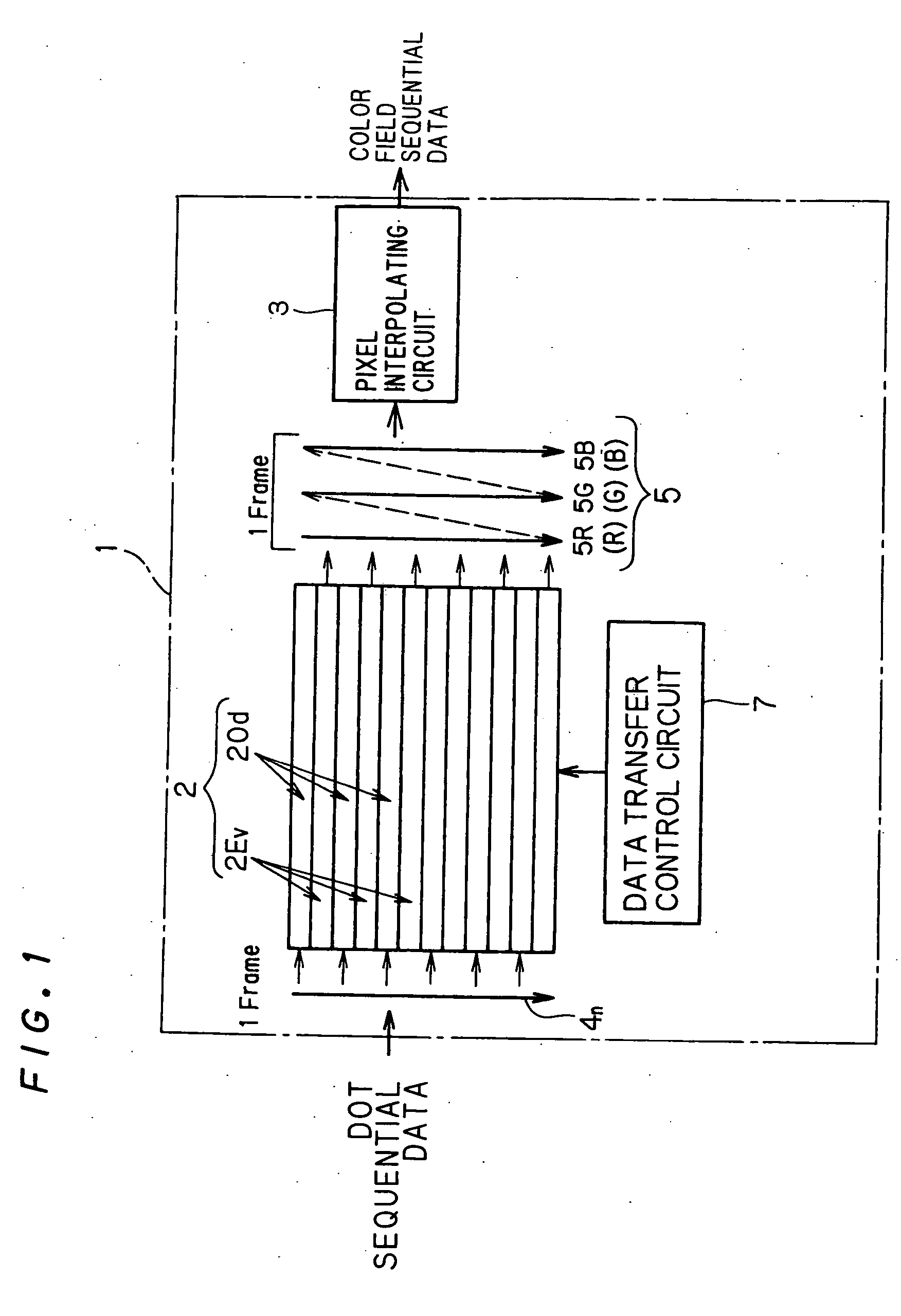
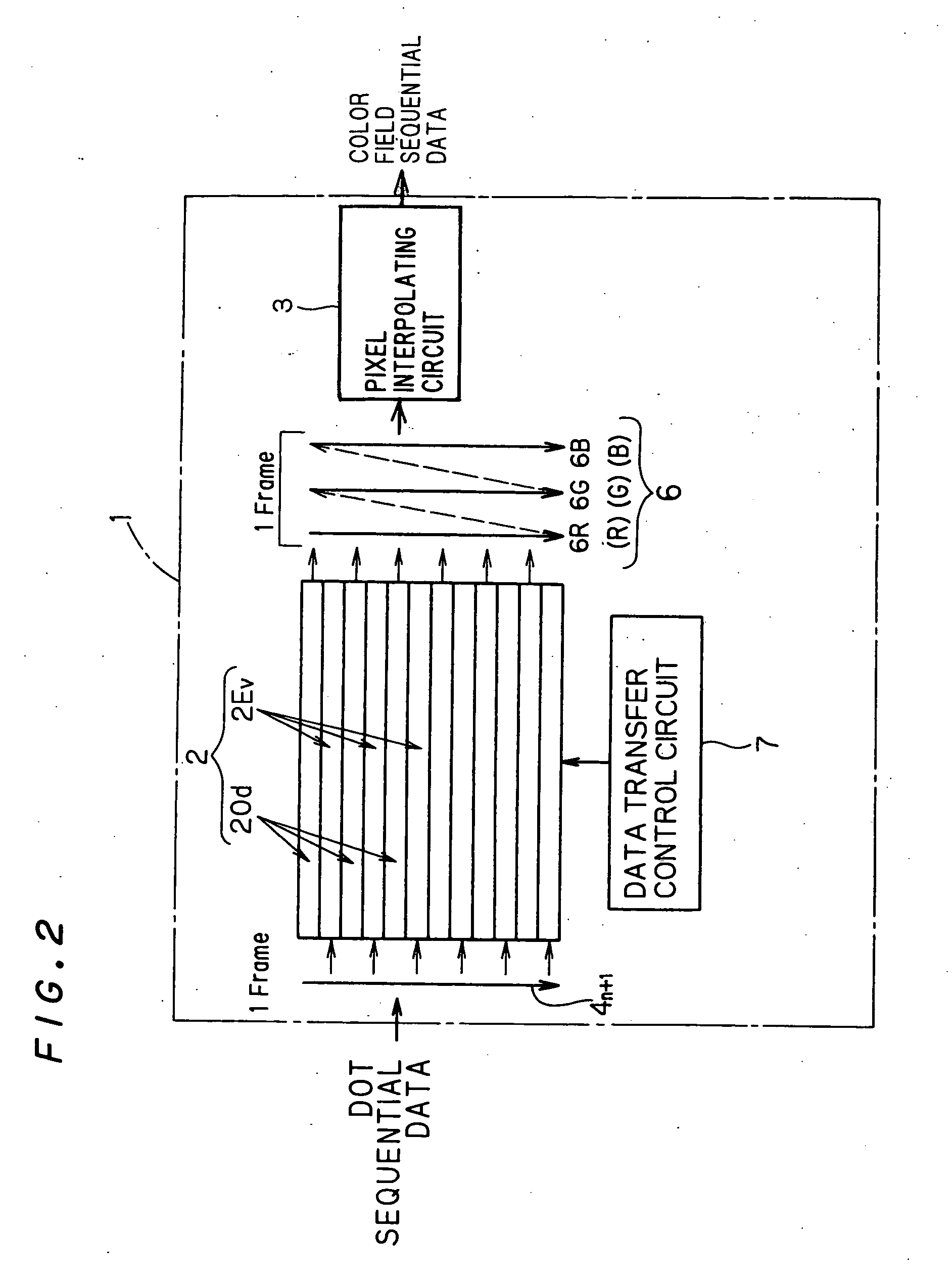
[0138]FIGS. 1 and 2 are block diagrams that show a schematic construction of an image conversion device 1 in accordance with first preferred embodiment of the present invention. This image conversion device 1 is provided with an image storing unit 2 for storing dot sequential data consisting of color components of R, G, B, a data transfer control circuit 7 which carries out controlling operations to transfer dot sequential data to image storing unit 2 to store them therein and to read out the dot sequential data stored in image storing unit 2 in a color field sequential format so as to be transferred, and a pixel interpolating circuit 3 which carries out a pixel interpolating process on color field sequential data 5 or 6 that has been transferred from image storing unit 2. Here, such an image conversion device 1 is provided as an integrated circuit.

[0139] Image storing unit 2, which has a buffer area corresponding to approximately one frame, is provided with a first buffer area 2Od...

second preferred embodiment

[0150] Next, an explanation will be given of second preferred embodiment of the present invention. FIG. 4 is a block diagram that shows a schematic construction of an image conversion device 10 in accordance with second preferred embodiment of the present invention.

[0151] In addition to a construction of image conversion device 1 according to the above-mentioned first preferred embodiment, this image conversion device 10 is further provided with a first color space conversion circuit 11 for color-space-converting inputted dot sequential data, and a sub-sampling circuit 12 which carries out a sub-sampling process on the dot sequential data that have been color-space-converted in the first color space conversion circuit 11, an over sampling circuit 13 which carries out a reverse conversion to the sub-sampling (hereinafter, referred to an over-sampling) to the color field sequential data 16 read out from image storing unit 2, and a second color space conversion circuit 14 which return...

third preferred embodiment

[0156] Next, an explanation will be given of third preferred embodiment of the present invention. FIG. 6 is a block diagram that shows a schematic construction of an image conversion device 20 in accordance with third preferred embodiment of the present invention.

[0157] In addition to the construction of image conversion device 1 in accordance with the above-mentioned first preferred embodiment, this image conversion device 20 is provided with a comparison circuit 21 which compares inputted dot sequential data 17 with the dot sequential data stored in image storing unit 2, an intra-frame determining circuit 22 which makes a determination as to whether or not the inputted dot sequential data are coincident with the dot sequential data stored in image storing unit 2 on the frame basis based upon a comparison signal outputted by the comparison circuit 21 and an operation mode control circuit 23 which outputs a switching control signal for switching modes to either one of a motion pict...


PUM


Abstract

An image conversion device is provided with a first buffer area for storing either one of even field and odd field of inputted dot sequential data and a second buffer area for storing the other thereof. A data transfer control circuit controls in such a manner that, during a period in which one of the two fields is written in the first buffer area, the other field, stored in the second buffer area, is read out in a color field sequential format, and during a period in which the other field is written in the second buffer area, the other field, stored in the first buffer area, is read out in a color field sequential format. A pixel interpolating circuit carries out an insertion-interpolating process on the field read out from the image storing unit, and outputs the resulting data. Thus, it becomes possible to prevent color breaking at the time of displaying motion images on a color field sequential type display by using a buffer area having a capacity of one frame.

Description

BACKGROUND OF THE INVENTION [0001] 1. Field of the Invention [0002] The present invention relates to a data conversion circuit for converting a component array, etc. of image data in an image processing device such as a digital camera. [0003] 2. Description of the Related Art [0004]FIG. 44 is a block diagram that shows a schematic construction of a digital camera. In this digital camera, light that has passed through an optical system 500 is detected by a CCD image-pickup element 501 and converted to an analog signal. An analog signal processing unit 502 subjects the analog signal inputted from CCD image-pickup element 501 to a gain adjusting process and an A / D converting process so as to generate a digital signal (Raw Image Data), and outputs this signal to an image processing unit 503. An image processing unit 503 has subjected the raw image data to digital image processing such as a pixel interpolating process, an edge emphasizing process and a color space converting process and ...

Claims


Application Information

Patent Timeline
IPC IPC(8): H04N11/20H04N9/64
CPCH04N9/646
Inventor MATSUTANI, TAKASHISASAKI, GEN
Owner MEGACHIPS
Why Eureka
Try Eureka