Half-bridge package

Inactive Publication Date: 2006-02-16
INFINEON TECH AMERICAS
View PDF7 Cites 52 Cited by
  • Summary
  • Abstract
  • Description
  • Claims
  • Application Information

AI Technical Summary

Problems solved by technology

Thus, a prior art package consumes more footprint on a circuit board and would natur

Method used


Image

  • Half-bridge package
  • Half-bridge package
  • Half-bridge package

Examples


Example

DETAILED DESCRIPTION OF THE FIGURES

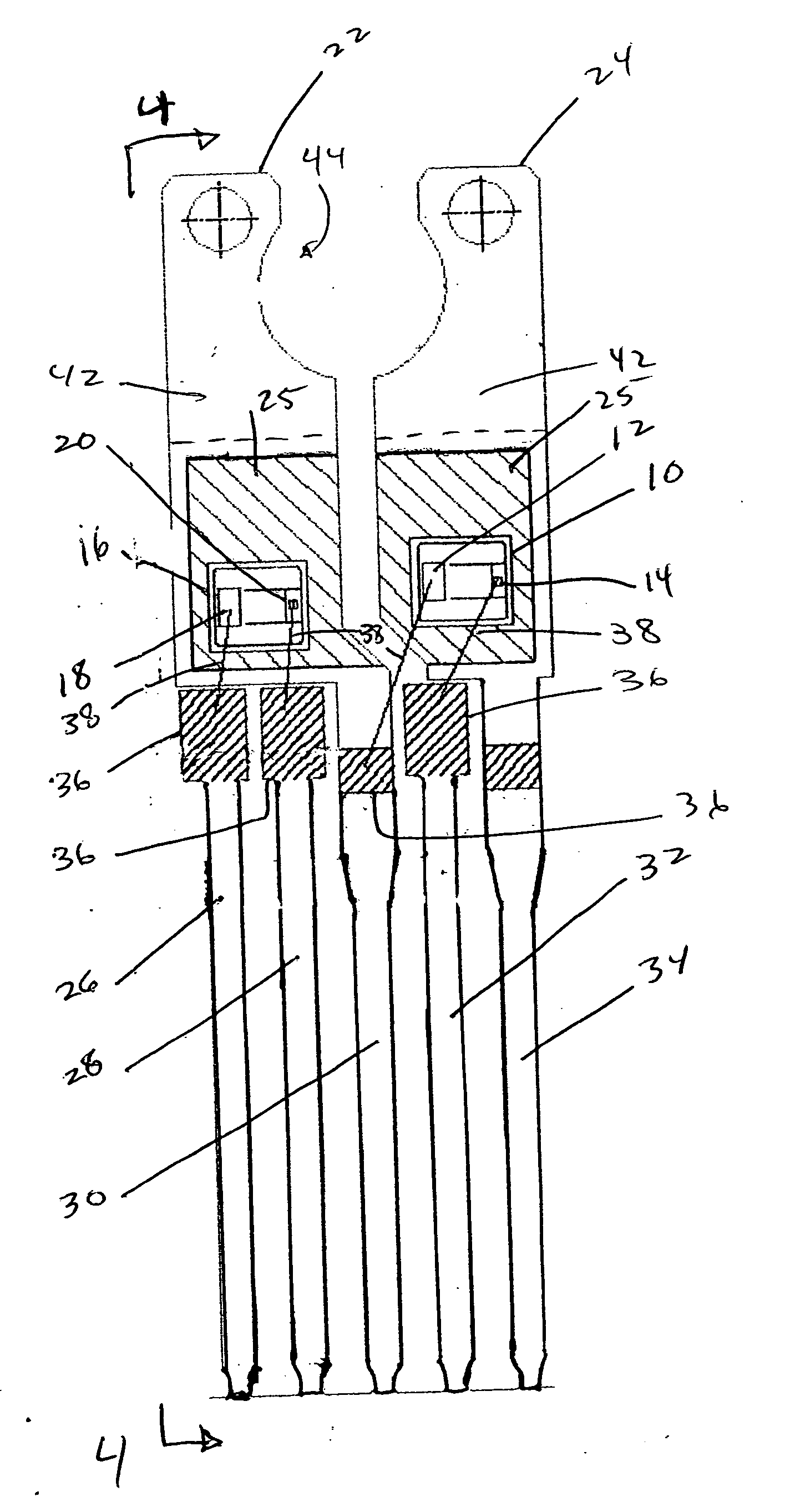
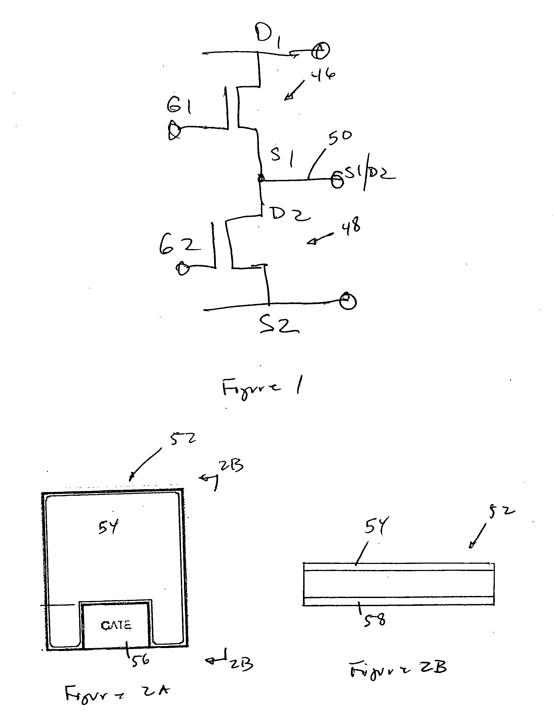
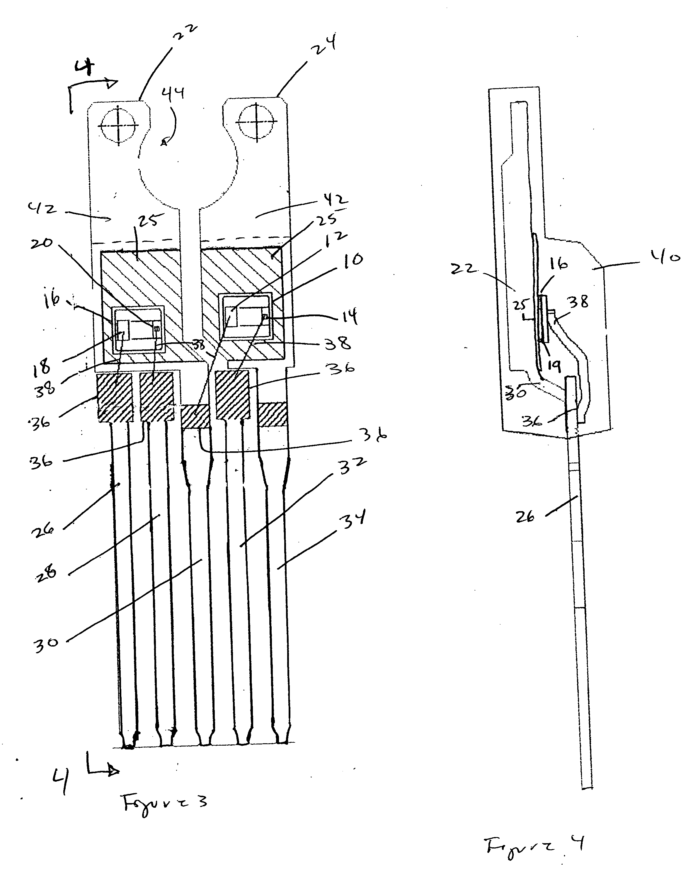
[0013] Referring to FIG. 3, a semiconductor package according to the present invention includes two power semiconductor devices arranged to form a half bridge. Specifically, a semiconductor package according to the present invention includes first semiconductor die 10 (high side) having a first power electrode 12 and a control electrode 14 on a surface thereof and a second power electrode on an opposing surface thereof; second semiconductor die 16 (low side) having a first power electrode 18 and a control electrode 20 on a surface thereof and a second power electrode 19 (see FIG. 4) on an opposing surface thereof; a split conductive pad arrangement including two isolated die pads 22, 24, each being electrically connected to a respective one of the second power electrodes by a conductive adhesive 25, such as solder, conductive epoxy or the like; and a plurality of electrically conductive leads 26, 28, 30, 32, 34 including at least one output lead 3...


PUM


Abstract

A semiconductor package which includes two power semiconductor die arranged in a half-bridge configuration.

Description

RELATED APPLICATION [0001] This application is based on and claims benefit of U.S. Provisional Application No. 60 / 600,503, filed Aug. 11, 2004, entitled COPAK HALF-BRIDGE MODULE, to which a claim of priority is hereby made and the disclosure of which is incorporated by reference. This application is related to U.S. patent application Ser. No. 10 / 988,443, filed Nov. 12, 2004, entitled LOW PROFILE PACKAGE HAVING MULTIPLE DIE.BACKGROUND OF THE INVENTION [0002] The present invention relates to semiconductor device packages and more particularly to co-packages. [0003] Half-bridge circuits are well known in the art of power supplies. Referring to FIG. 1, a half-bridge includes two power semiconductor die connected in series. For example, a typical half bridges includes a first power MOSFET 46 (typically referred to as the high side switch or high side) having a drain side thereof electrically connectable to the bus, and the source side thereof electrically connected to the drain side of s...

Claims


Application Information

Patent Timeline
IPC IPC(8): H01L31/111
CPCH01L23/49562H01L2224/32245H01L2224/48091H01L2224/48247H01L2224/48472H01L2224/49171H01L2924/01013H01L2924/01029H01L2924/01079H01L2924/01082H01L2924/13055H01L2924/13091H01L2924/30107H01L24/40H01L2224/73265H01L2924/1305H01L24/48H01L24/49H01L2924/01033H01L2924/01047H01L2924/00014H01L2924/00H01L2924/00012H01L2924/181H01L2224/40245H01L24/73H01L2224/45015H01L2224/45124H01L2224/45147H01L2224/45144H01L24/45H01L2224/45014H01L2224/37144H01L2224/37124H01L2224/37147H01L2224/83801H01L2224/8385H01L24/37H01L2224/73221H01L2924/2075H01L2924/206
Inventor PAVIER, MARKDUBHASHI, AJITCONNAH, NORMAN G.CEREZO, JORGE
Owner INFINEON TECH AMERICAS
Why Eureka
Try Eureka