Method for designing semiconductor integrated circuit, semiconductor integrated circuit and program for designing same

a technology of reset signal and integrated circuit, which is applied in the direction of program control, generating/distributing signals, instruments, etc., can solve the problems of more severe timing constraints on reset signals, inability to adopt tree structures, and inability to meet time constraints (clock cycles or the like) sometimes to design reset signals, etc., to achieve the effect of facilitating the design of reset signals, reducing product cost, and reducing development period

a technology of reset signal and integrated circuit, which is applied in the direction of program control, generating/distributing signals, instruments, etc., can solve the problems of more severe timing constraints on reset signals, inability to adopt tree structures, and inability to meet time constraints (clock cycles or the like) sometimes to design reset signals, etc., to achieve the effect of facilitating the design of reset signals, reducing product cost, and reducing development period

US20060117285A1Inactive Publication Date: 2006-06-01SOCIONEXT INC

Image

  • Method for designing semiconductor integrated circuit, semiconductor integrated circuit and program for designing same
  • Method for designing semiconductor integrated circuit, semiconductor integrated circuit and program for designing same
  • Method for designing semiconductor integrated circuit, semiconductor integrated circuit and program for designing same

Examples


Embodiment Construction

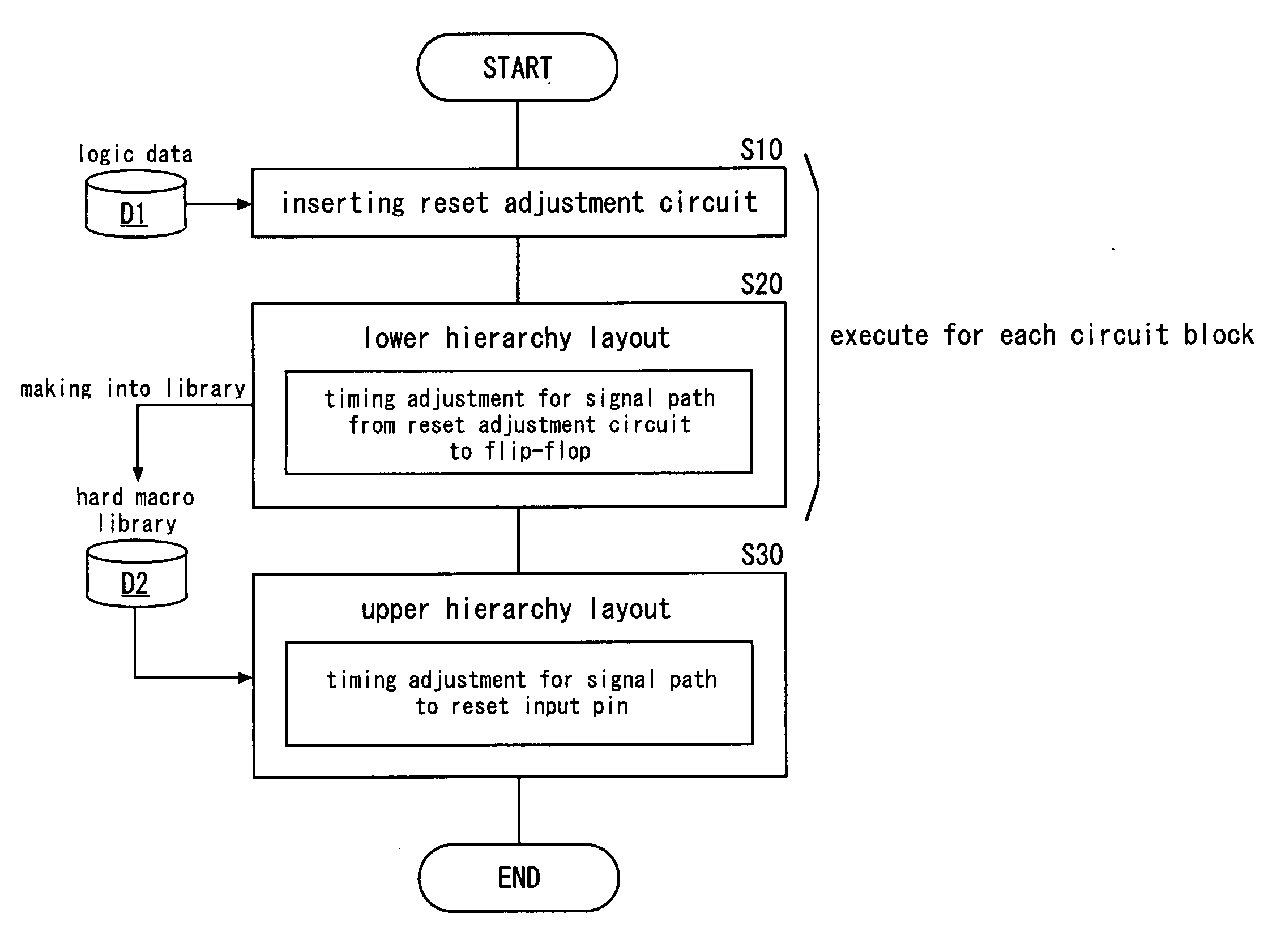
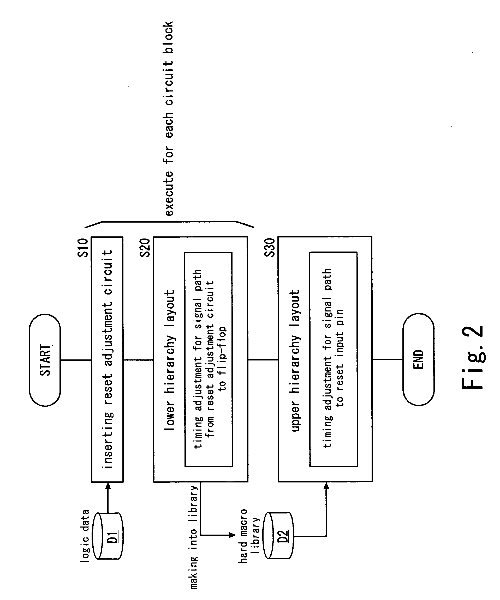
[0032] In a preferable example of the first or the second aspect of the present invention, a first synchronization circuit of the reset adjustment circuit outputs as a first internal signal the reset signal from the reset input pin, in synchronization with the clock signal. A logic operation circuit of the reset adjustment circuit activates an internal reset signal to be supplied to the flip-flips, in synchronization with the activation transition of the reset signal. The logic operation circuit deactivates the internal reset signal in synchronization with deactivation transition of the first internal signal. Therefore, the activation timing of the internal reset signal is the same as that of the reset signal, and is irrespective of the clock signal. On the other hand, the deactivation timing of the internal reset signal is the same as that of the first internal signal and is synchronous with the clock signal. Therefore, if the timing adjustment using the clock signal as a reference...


PUM


Abstract

In lower hierarchy design in which a plurality of circuit blocks are independently designed, a reset adjustment circuit propagating deactivation transition of a reset signal to flip-flops in synchronization with a clock signal is inserted immediately after a reset input pin in each circuit block, and timing adjustment using the clock signal as a reference is implemented for signal paths of the reset signal from the reset adjustment circuit to the flip-flops. In upper hierarchy design in which an entire semiconductor integrated circuit is designed, timing adjustment using the clock signal as a reference is implemented for signal paths of the reset signal, according to setup times and hold times of the reset signal that are prescribed respectively for the reset input pins of the circuit blocks.

Description

CROSS REFERENCE TO RELATED APPLICATION [0001] This application is based upon and claims the benefit of priority from Japanese Patent Application No. 2004-341676, filed on Nov. 26, 2004, the entire contents of which are incorporated herein by reference. BACKGROUND OF THE INVENTION [0002] 1. Field of the Invention [0003] The present invention relates to a semiconductor integrated circuit, and more particularly, to a technique of designing a reset signal in the semiconductor integrated circuit. [0004] 2. Description of the Related Art [0005] In designing a large-scale LSI, as a method to effectively utilize intellectual property and reduce a design period, known is hierarchical design (hierarchical layout design) in which physical design (layout design) of each lower hierarchy block is independently implemented, and physical design of the entire LSI (upper hierarchy) is implemented, using the lower hierarchy blocks (including hard macro which is a library of layout data) whose physical...

Claims


Application Information

Patent Timeline
01 Jun 2006
Publication
US20060117285A1
IPC
G06F17/50; G06F1/12; G06F1/04
CPC
G06F1/24; G06F17/505; G06F17/5068; G06F30/39; G06F30/327
Inventors
KOSUGI, NAOTO; DAIJO, JIRO