Method of collector formation in BiCMOS technology
a collector and bicmos technology, applied in the field of bipolar and complementary metal oxide semiconductor (bicmos) technology, can solve the problems of serious device operational limitations, double collector layout design limitations in improving npn performance, etc., and achieve the effect of minimal disturbance of the bicmos process flow and lower resistance subcollector
- Summary
- Abstract
- Description
- Claims
- Application Information
AI Technical Summary
Benefits of technology
Problems solved by technology
Method used
Image
Examples
first embodiment
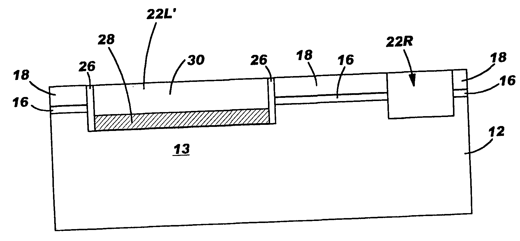
[0057] After this etch which extends the opening 35, nitride or oxynitride spacers 26 are formed on the exposed sidewalls of the extended opening 35. The resultant structure including the extended opening 35 and the spacers 26 is shown in FIG. 2B. Note that the spacers 26 are formed as described above in the present invention.
[0058] The remaining first trench dielectric of shallow trench isolation region 22L is then removed utilizing a wet etch process that selectively removes the first trench dielectric material, i.e., oxide, stopping on the surface of substrate 12. A lateral etch may now be optionally performed which provides undercut region 36 in the extended opening 35. The lateral undercut 36 is preferred since it ensures that the silicide will be in closer proximity to the emitter region. The lateral etch may be performed by a wet chemical etch such as HF-containing agent.
second embodiment
[0059] A refractory metal layer is then formed as described above. FIG. 2D shows an embodiment in which the refractory metal layer (designated by reference numeral 27) is formed by a non-selective deposition process. Although the drawing depicts the formation of the refractory metal layer 27 by a non-selective deposition method, the second embodiment also contemplates the selective deposition method described above as well.
[0060] In the case illustrated, the refractory metal layer 27 that is outside of opening 35 is then removed providing the structure shown in FIG. 2E. The processing steps described above, i.e., silicide formation, and second trench dielectric material 30 formation and planarization, are then performed to provide a substantially planarized structure similar to the one shown in FIG. 1F except for the presence of the undercut region that is filled with silicide. CMOS processing and bipolar transistor formation can then be performed on the substantially planarized str...
PUM
| Property | Measurement | Unit |
|---|---|---|
| temperature | aaaaa | aaaaa |
| temperature | aaaaa | aaaaa |
| thickness | aaaaa | aaaaa |
Abstract
Description
Claims
Application Information


