Method of collector formation in BiCMOS technology

a collector and bicmos technology, applied in the field of bipolar and complementary metal oxide semiconductor (bicmos) technology, can solve the problems of serious device operational limitations, double collector layout design limitations in improving npn performance, etc., and achieve the effect of minimal disturbance of the bicmos process flow and lower resistance subcollector

Active Publication Date: 2006-02-21
ELPIS TECH INC
View PDF9 Cites 13 Cited by
  • Summary
  • Abstract
  • Description
  • Claims
  • Application Information

AI Technical Summary

Benefits of technology

[0009]The present invention provides a heterobipolar transistor (HBT) having a lower Rc than conventional HBTs by providing a buried refractory metal silicide underneath the shallow trench isolation region on the subcollector of the device. Refractory metal silicides such as, for example, tungsten silicide, can survive the subsequent high-temperature thermal cycles in CMOS and bipolar modules, while offering a lower resistance subcollector, and minimally disturbing the BiCMOS process flow.

Problems solved by technology

As the vertical dimensions of the bipolar transistor are scaled more and more, serious device operational limitations have been encountered.
Thus, the double collector layout design has its limitation in improving NPN performance.

Method used


Image

  • Method of collector formation in BiCMOS technology
  • Method of collector formation in BiCMOS technology
  • Method of collector formation in BiCMOS technology

Examples


first embodiment

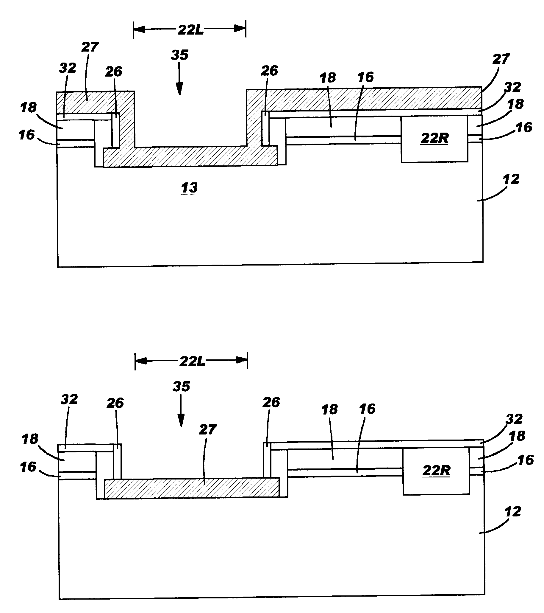
[0057]After this etch which extends the opening 35, nitride or oxynitride spacers 26 are formed on the exposed sidewalls of the extended opening 35. The resultant structure including the extended opening 35 and the spacers 26 is shown in FIG. 2B. Note that the spacers 26 are formed as described above in the present invention.

[0058]The remaining first trench dielectric of shallow trench isolation region 22L is then removed utilizing a wet etch process that selectively removes the first trench dielectric material, i.e., oxide, stopping on the surface of substrate 12. A lateral etch may now be optionally performed which provides undercut region 36 in the extended opening 35. The lateral undercut 36 is preferred since it ensures that the silicide will be in closer proximity to the emitter region. The lateral etch may be performed by a wet chemical etch such as HF-containing agent.

second embodiment

[0059]A refractory metal layer is then formed as described above. FIG. 2D shows an embodiment in which the refractory metal layer (designated by reference numeral 27) is formed by a non-selective deposition process. Although the drawing depicts the formation of the refractory metal layer 27 by a non-selective deposition method, the second embodiment also contemplates the selective deposition method described above as well.

[0060]In the case illustrated, the refractory metal layer 27 that is outside of opening 35 is then removed providing the structure shown in FIG. 2E. The processing steps described above, i.e., silicide formation, and second trench dielectric material 30 formation and planarization, are then performed to provide a substantially planarized structure similar to the one shown in FIG. 1F except for the presence of the undercut region that is filled with silicide. CMOS processing and bipolar transistor formation can then be performed on the substantially planarized struc...


PUM

PropertyMeasurementUnit
thicknessaaaaaaaaaa
thicknessaaaaaaaaaa
thicknessaaaaaaaaaa

Abstract

A heterobipolar transistor (HBT) for high-speed BiCMOS applications is provided in which the collector resistance, Rc, is lowered by providing a buried refractory metal silicide layer underneath the shallow trench isolation region on the subcollector of the device. Specifically, the HBT of the present invention includes a substrate including at least a subcollector; a buried refractory metal silicide layer located on the subcollector; and a shallow trench isolation region located on a surface of the buried refractory metal silicide layer. The present invention also provides a method of fabricating such a HBT. The method includes forming a buried refractory metal silicide underneath the shallow trench isolation region on the subcollector of the device.

Description

FIELD OF THE INVENTION[0001]The present invention relates generally to bipolar and complementary metal oxide semiconductor (BiCMOS) technology and, more particularly to a bipolar transistor (NPN or PNP) that includes a buried refractory metal silicide layer underneath a shallow trench isolation region on the subcollector of the device. The bipolar transistor of the present invention exhibits reduced collector resistance, Rc, therefore it is applicable for use in high-speed applications. The present invention is also related to a method of fabricating the inventive bipolar transistor that includes the buried refractory metal silicide layer underneath the shallow trench isolation region on the subcollector of the device.BACKGROUND OF THE INVENTION[0002]Bipolar transistors are electronic devices with two p-n junctions that are in close proximity to each other. A typical bipolar transistor has three device regions: an emitter, a collector, and a base disposed between the emitter and the...

Claims


Application Information

Patent Timeline
Patent Type & Authority Patents(United States)
IPC IPC(8): H01L31/072H01L31/0328H01L31/0336H01L31/109
CPCH01L29/66318H01L29/66242H01L29/0821H01L21/8249H01L27/0623H01L29/737
Inventor GEISS, PETER J.GRAY, PETER B.JOSEPH, ALVIN J.LIU, QIZHI
Owner ELPIS TECH INC
Why Eureka
Try Eureka