Flat panel display

a technology for flat panels and displays, applied in the direction of discharge tubes/lamp details, discharge tubes luminescnet screens, electric discharge lamps, etc., can solve the problems of increasing problems, reducing image quality, and uneven power supplied to each of the pixels, so as to prevent a voltage drop of driving power and improve the characteristics of electronic devices

Active Publication Date: 2006-11-30
SAMSUNG DISPLAY CO LTD
View PDF8 Cites 58 Cited by
  • Summary
  • Abstract
  • Description
  • Claims
  • Application Information

AI Technical Summary

Benefits of technology

[0011] The present invention provides a flat panel display that prevents a voltage drop of a driving power and improves the characteristics of electronic devices in a circuit region where various circuit devices are mounted and electronic devices included in a pixel region.

Problems solved by technology

The voltage of the power supplied to each of the pixels is not uniform due to a voltage drop in Vdd lines.
As a result, non-uniform brightness can occur resulting in the degradation of the image quality.
This problem is increased when the screen is large and when there are more capacitors.

Method used


Image

  • Flat panel display
  • Flat panel display
  • Flat panel display

Examples


Embodiment Construction

[0031] The present invention is described more fully below with reference to the accompanying drawings in which exemplary embodiments of the present invention are shown.

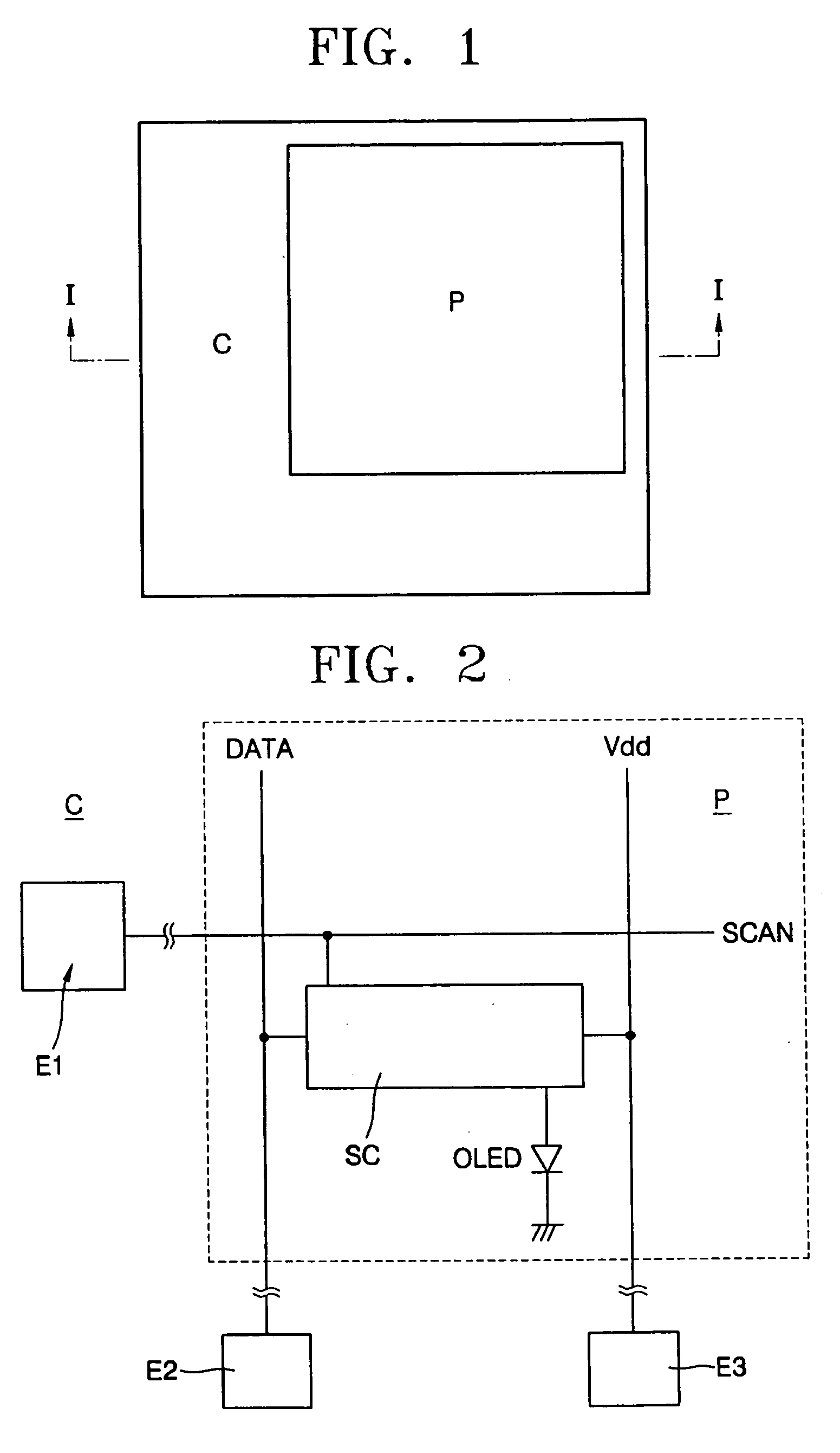
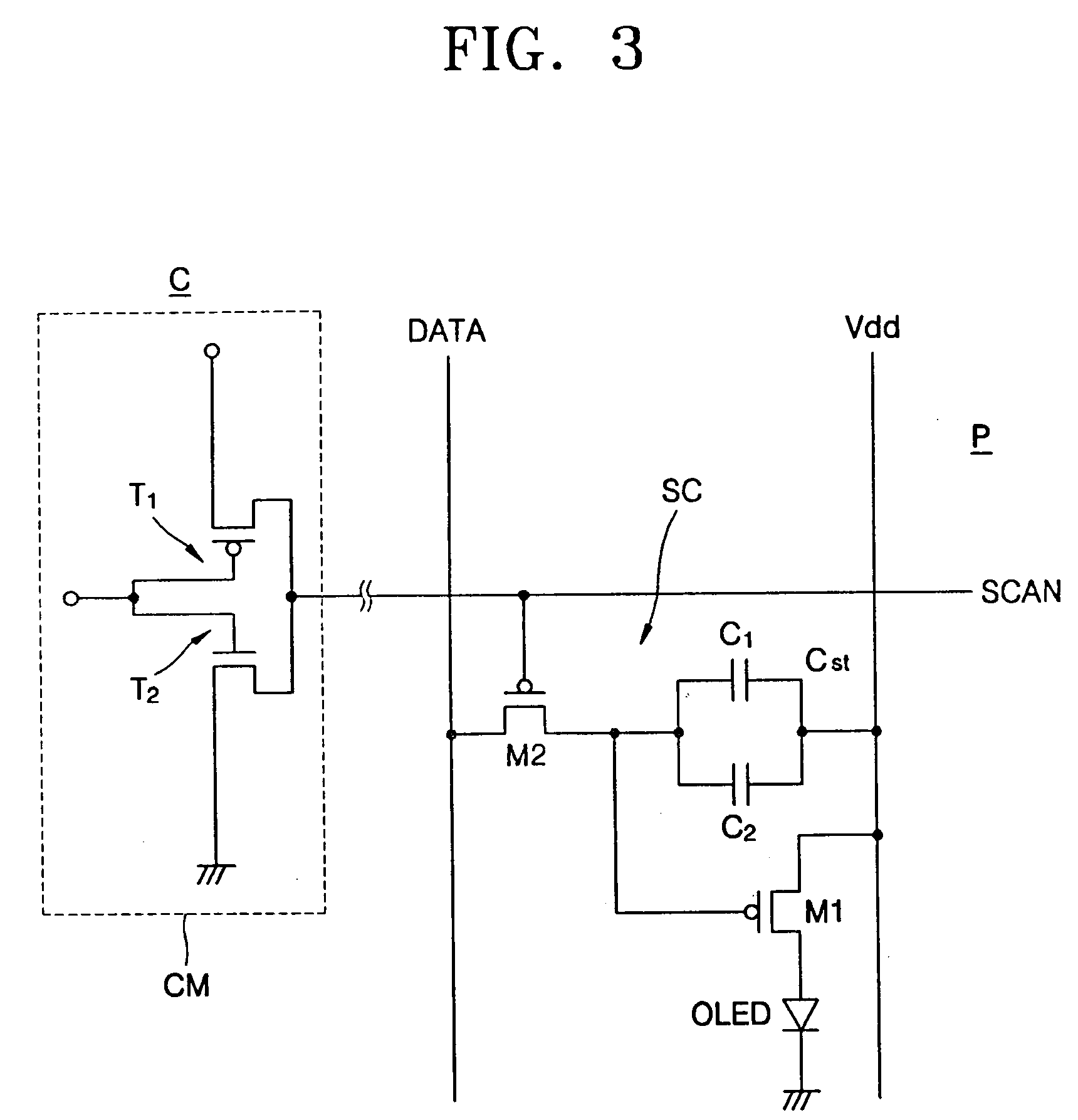
[0032]FIG. 1 is a plan view of an Active Matrix (AM) Organic Light Emitting Display (OLED) of a flat panel display according to an embodiment of the present invention. Referring to FIG. 1, the OLED includes a pixel region P and a circuit region C located on edges of the pixel region P.

[0033] The pixel region P includes a plurality of pixels, and each pixel includes an organic light emitting device such as an organic Light Emitting Diode (LED). In a full color OLED, red R, green G, and blue B color pixels are arranged in various patterns, such as a line shape, a mosaic shape, or a lattice shape, and the OLED can be a mono color flat panel display.

[0034] The circuit region C includes electronic devices that control the organic LEDs located in pixels of the pixel region P, and circuits in the circuit region C control...


PUM


Abstract

A flat panel display that can prevent a voltage drop of a driving power and, at the same time, minimizes the characteristic reduction of electronic devices located in a circuit region where various circuit devices are located includes: a substrate; an insulating film arranged on the substrate; a pixel region including at least one light emitting diode, the pixel region arranged on the insulating film and adapted to display an image; a circuit region arranged on the insulating film and including electronic devices adapted to control signals supplied to the pixel region; and a conductive film interposed between the substrate and the insulating film in a region corresponding to the pixel region and electrically connected to one electrode of the light emitting diode.

Description

CLAIM OF PRIORITY [0001] This application makes reference to, incorporates the same herein, and claims all benefits accruing under 35 U.S.C.§119 from the two applications both of which are entitled FLAT PANEL DISPLAY DEVICE and earlier filed in the Korean Intellectual Property Office on the 28th of May 2005 and the 23rd of June 2005 and there, duly assigned Ser. Nos. 10-2005-0045298 and 10-2005-0054369, respectively. BACKGROUND OF THE INVENTION [0002] 1. Field of the Invention [0003] The present invention relates to a flat panel display, and more particularly, to a flat panel display that prevents the voltage drop of a driving power and minimizes a reduction of characteristics of electronic devices included in a circuit region where various circuit devices are mounted. [0004] 2. Description of the Related Art [0005] A lot of research into manufacturing super slim and flexible flat panel displays, such as Organic Light Emitting Displays (OLEDs) or Thin Film Transistor-Liquid Crystal ...

Claims


Application Information

Patent Timeline
Patent Type & Authority Applications(United States)
IPC IPC(8): H01J1/62H01J63/04
CPCH01L27/3276H01L27/3265H10K59/1216H10K59/131
Inventor KOO, JAE-BONJEONG, JAE-KYEONGSHIN, HYUN-SOOMO, YEON-GON
Owner SAMSUNG DISPLAY CO LTD
Why Eureka
Try Eureka