Thyristor-based semiconductor memory device with back-gate bias

Inactive Publication Date: 2009-08-11
T RAM ASSIGNMENT FOR THE BENEFIT OF CREDITORS LLC +1
View PDF18 Cites 24 Cited by
  • Summary
  • Abstract
  • Description
  • Claims
  • Application Information

AI Technical Summary

Benefits of technology

[0009]According to an embodiment of the present invention, a thyristor-based semiconductor memory device may be formed on an SOI wafer. An underlying supporting substrate may be doped with a high density of impurity to allow efficient back-gate control of the gain of bipolar devices constituting a

Problems solved by technology

For example, a holding current larger than a few nano-Amperes per cell could significantly impact its power dissipation and limit the maximum capacity of a thyristor-based memory within, for example, an expanded memory array solution.
A thyristor may be vulnerable to error responsive to various adverse environmental conditions such as noise, light, anod

Method used


Image

  • Thyristor-based semiconductor memory device with back-gate bias
  • Thyristor-based semiconductor memory device with back-gate bias
  • Thyristor-based semiconductor memory device with back-gate bias

Examples


Example

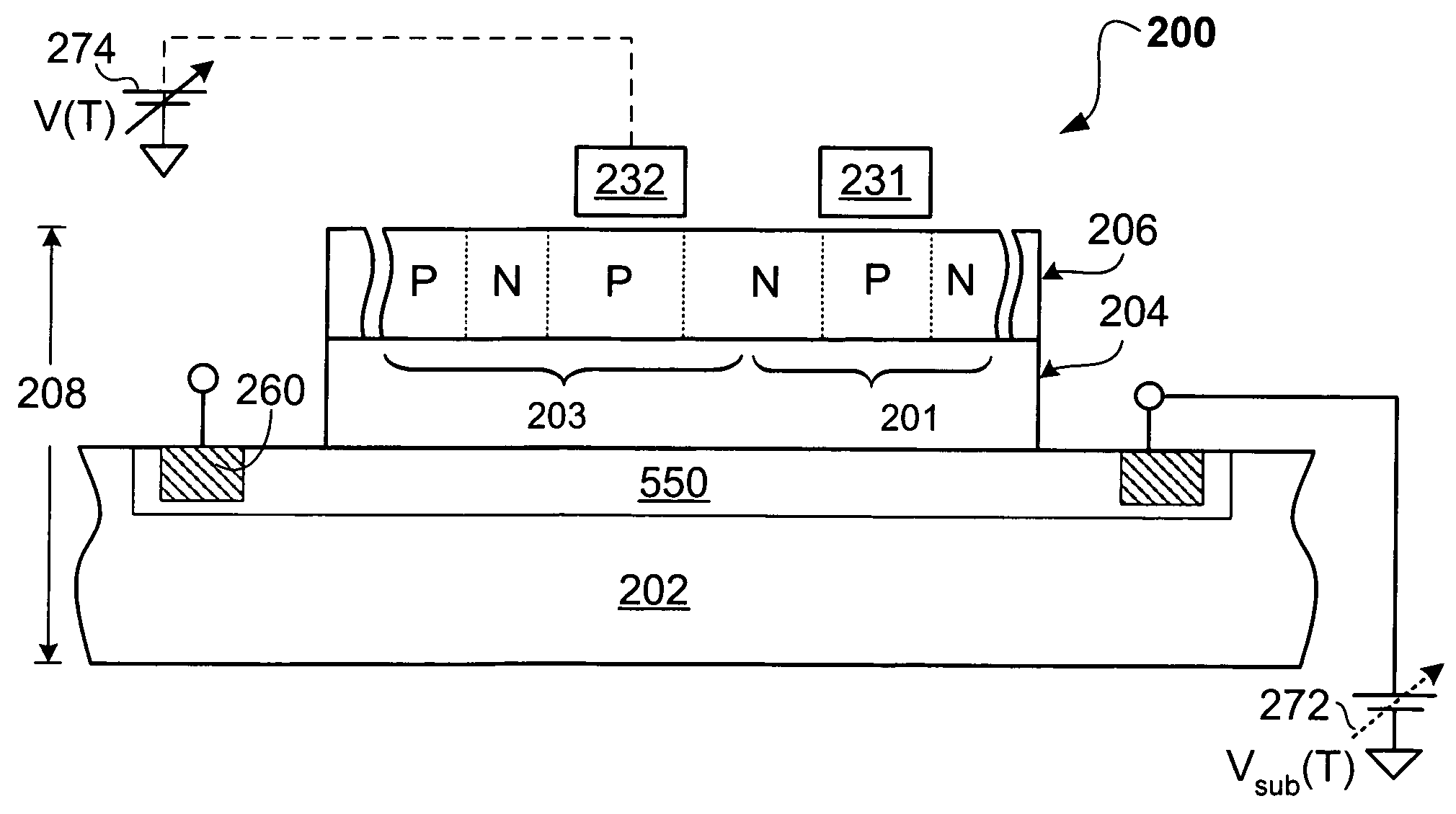
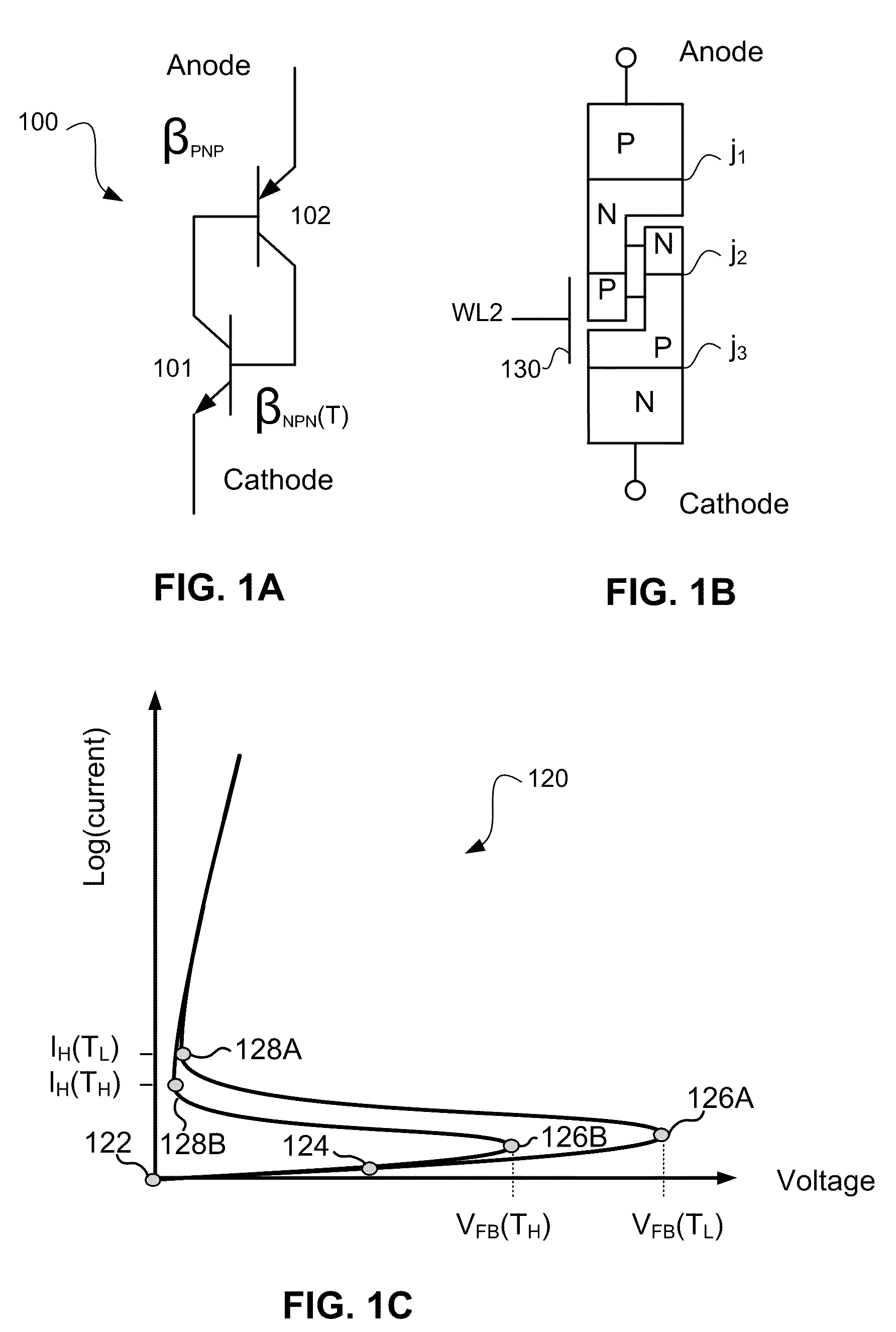
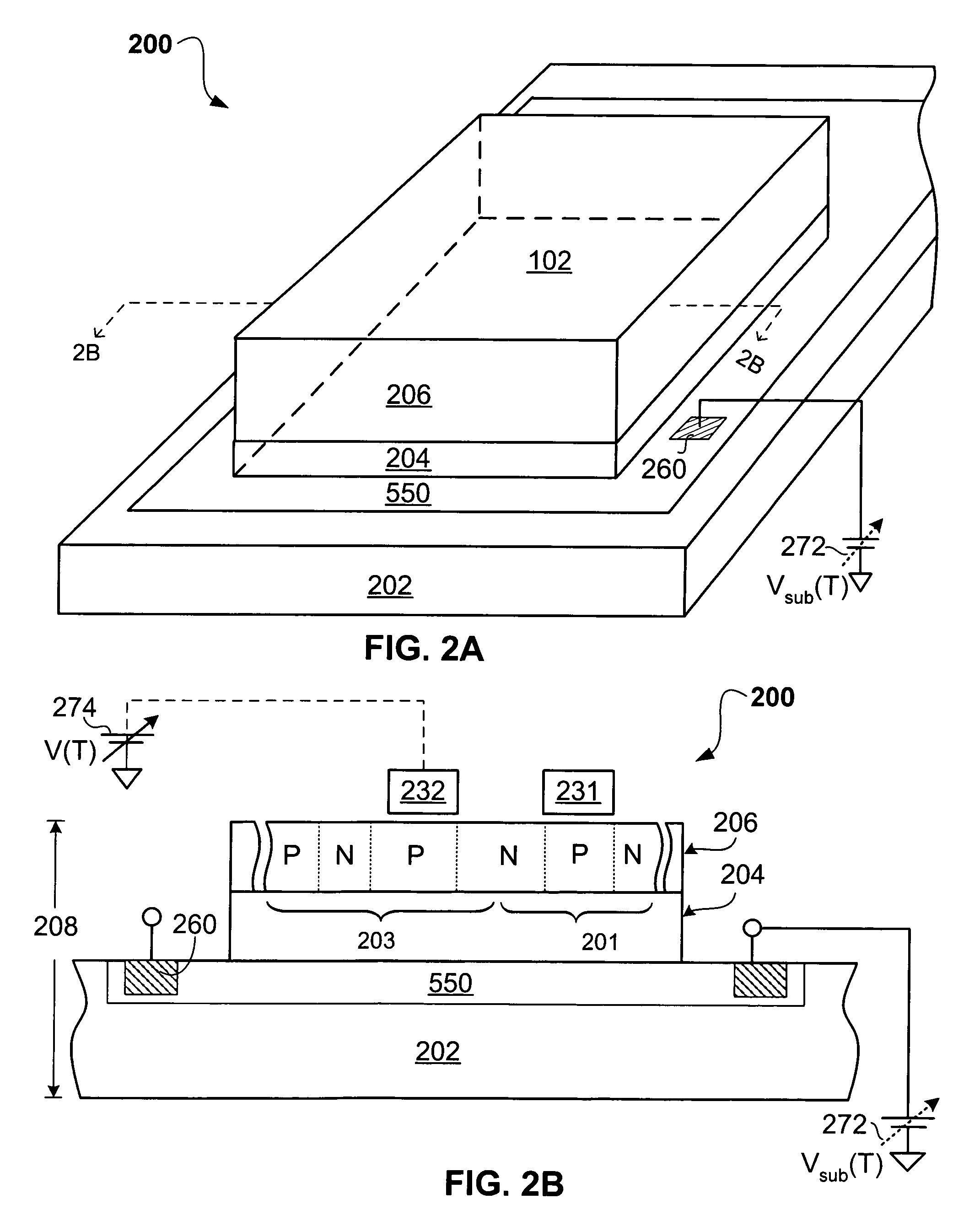
[0029]In the description that follows, readily established procedures for the exemplary embodiments may be disclosed in simplified form (e.g., simplified block diagrams and / or simplified description) to avoid obscuring an understanding of the embodiments with excess detail and where persons of ordinary skill in this art can readily understand their structure and formation by way of the drawings and disclosure. For the same reason, identical components may be given the same reference numerals, regardless of whether they are shown in different embodiments of the invention.

[0030]Embodiments of the present invention may be applicable to a variety of different types of thyristor-based memories, and have been found to be particularly useful for such devices benefiting from improved stability in the presence of disturbing environmental conditions such as high temperature, noise, light and voltage changes. While the present invention is not necessarily limited to such devices, various aspec...


PUM


Abstract

In accordance with an embodiment of the present invention, a thyristor-based semiconductor memory device may comprise an array of thyristor-based memory formed in an SOI wafer. A supporting substrate may be formed with a density of dopants sufficient to assist delivery of a bias level to the backside of an insulating layer beneath a thyristor. Such conductivity within the substrate may allow reliable back-gate control for the gain of a component bipolar device of the thyristor.

Description

RELATED DATA[0001]This application is related to; and U.S. patent application Ser. No. 10 / 741,539 filed on Dec. 12, 2003, now U.S. Pat. No. 7,078,739 issued Jul. 18, 2006 (Adaptive gate bias for improving temperature stability of thyristor-based memory), which is a continuation-in-part of U.S. patent application Ser. No. 10 / 706,162, filed on Nov. 12, 2003, now U.S. Pat. No. 7,304,327 (Thyristor Circuit and Approach for Temperature Stability); the specifications of which are hereby incorporated by reference.BACKGROUND[0002]The present invention is directed to semiconductor devices and, more specifically, to thyristor-based memory devices and their fabrication on SOI wafers.[0003]The semiconductor industry seems to continually strive for integrated circuits of greater density and complexity and, at the same time, seek reduced power consumption and package size. Recent advances, e.g., have brought forward single-die microprocessors with many millions of transistors that may operate at ...

Claims


Application Information

Patent Timeline
IPC IPC(8): H01L29/74
CPCH01L21/84H01L27/1027H01L29/7436H01L27/1203H01L27/105
Inventor ERSHOV, MAXIM
Owner T RAM ASSIGNMENT FOR THE BENEFIT OF CREDITORS LLC
Why Eureka
Try Eureka