Electroluminescence display device

a display device and electroluminescent technology, applied in the direction of static indicating devices, discharge tubes luminescnet screens, instruments, etc., can solve the problems of significant increase in cost, difference in light emission intensity of organic el elements, degradation of display quality, etc., to reduce the potential drop on the drive line in the display region, the difference in the potential drop along the horizontal scan direction, and the effect of reducing the potential drop

Active Publication Date: 2006-12-21
SANYO ELECTRIC CO LTD
View PDF4 Cites 18 Cited by
  • Summary
  • Abstract
  • Description
  • Claims
  • Application Information

AI Technical Summary

Benefits of technology

[0019] With this structure, an intermediate position, along the horizontal scan direction, of the trunk line, which is provided along the horizontal scan direction of the display region, is connected to the common connection line from the external connection terminal instead of a position on the trunk line closest to the external connection terminal. Thus, a uniform drive current can be supplied to pixels at any position along the horizontal scan direction regardless of a distance from the external terminal; variation in the potential drop on the drive line in the display region, in particular, a difference in the potential drop along the horizontal scan direction, can be reduced; and potential drop itself can be reduced. In this manner, difference in light emission intensities among pixels at right and left positions in the display region can be minimized.

Problems solved by technology

This is because the change of layout or the like may involve a change of masks which are used for forming the element and line and re-examination of the characteristics, which result in significant increase in cost.
Such a difference in potential leads to a potential difference in corresponding power supply lines PL, resulting in different currents flowing through the organic EL elements depending on the position of the organic EL element on the panel, which is in turn recognized as a difference in the light emission intensity of the organic EL element and degradation of the display quality.

Method used


Image

  • Electroluminescence display device
  • Electroluminescence display device
  • Electroluminescence display device

Examples


Embodiment Construction

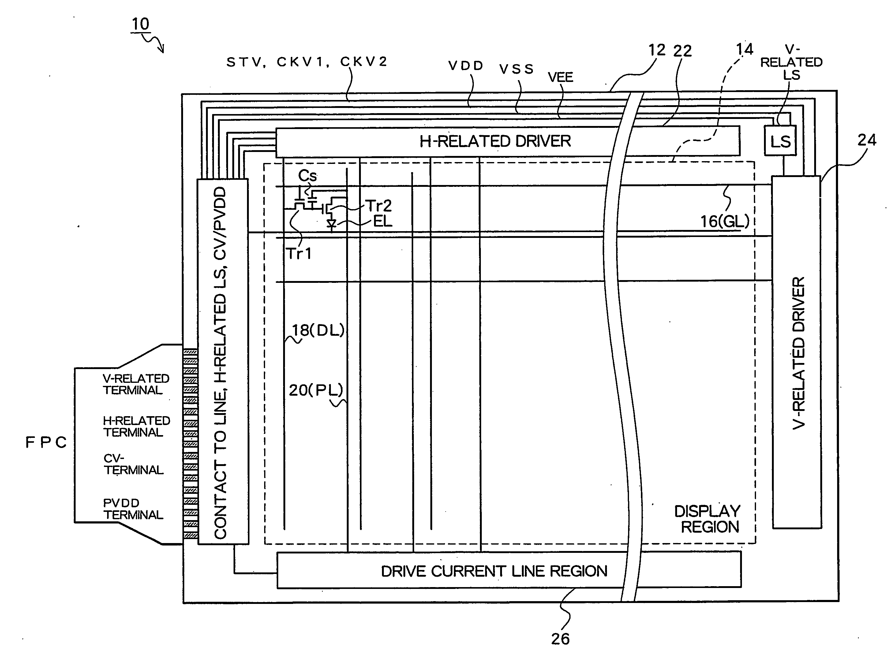
[0030] Preferred embodiments of the present invention will now be described referring to the drawings. FIG. 3 is a diagram schematically showing a panel layout of a display portion, circuits, and a line in an organic EL display device 10 according to a preferred embodiment of the present invention. A display region 14 is formed on a panel substrate 12 with a plurality of pixels arranged in a matrix form. In the display region 14 of the panel substrate 12, a gate line 16 (GL) to which a selection signal is sequentially output is formed along a horizontal scan (row) direction of the matrix and a data line 18 (DL) to which a data signal is output and a power supply line 20 (PL) for supplying a drive current from an operational power supply (PVDD) to an organic EL element which is an element to be driven are formed along a vertical scan (column) direction.

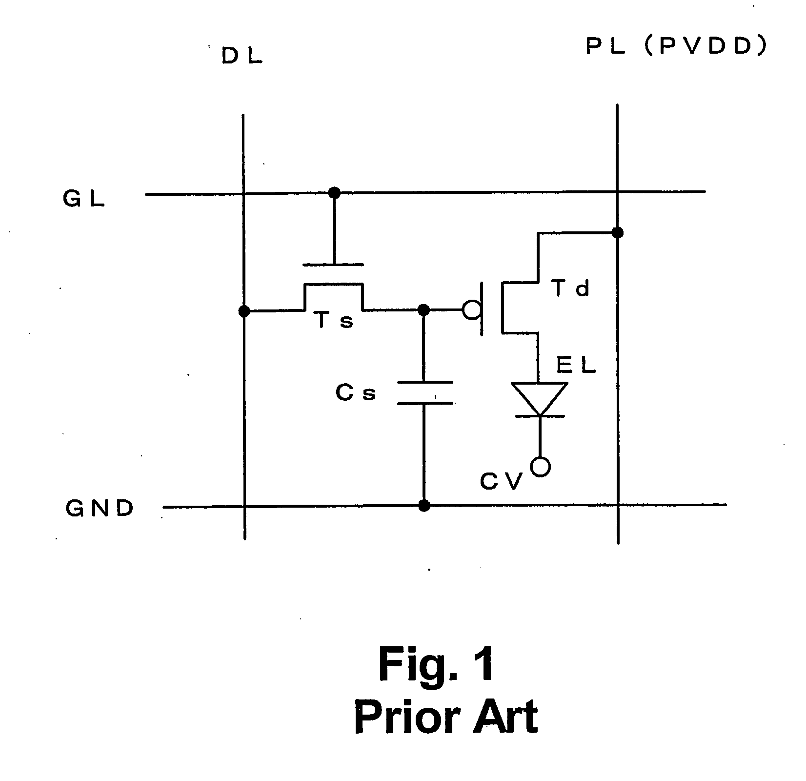
[0031] Each pixel is approximately provided at a region defined by these lines and comprises, as circuit elements, an organic EL ele...


PUM


Abstract

A display portion in which pixels are arranged in a matrix is formed on a display panel and a drive current line, which supplies a drive current from a terminal formed at a side along a column direction to a display element in each pixel, includes a branch line provided for each column of the display portion and along each column of the display portion; a trunk line to which the branch line is connected and which extends along a row direction at a peripheral portion at a lower side of the display portion; and a connection line which connects the trunk line and the terminal. The connection line is separated from a region of the trunk line near the terminal by a slit provided from a side of the trunk line near the terminal to a side of the trunk line distanced from the terminal and extends in parallel to the region of the trunk line near the terminal at the peripheral portion at the lower side of the display portion from a region in which the terminal is formed. The connection line is connected to the trunk line at an intermediate position of the peripheral portion at the lower side of the display portion along the row direction. A length of the slit and a width of the region of the trunk line near the terminal are optimized to inhibit brightness variation within the display portion.

Description

CROSS-REFERENCE TO RELATED APPLICATIONS [0001] The entire disclosure of Japanese Patent Application Nos. 2005-179083 and 2006-154839 including specification, claims, drawings, and abstract is incorporated herein by reference. BACKGROUND OF THE INVENTION [0002] 1. Field of the Invention [0003] The present invention relates to a line in a display device which uses a current-driven element, such as, for example, an organic electroluminescence element (hereinafter referred to as “organic EL element”), as a display element in each pixel. [0004] 2. Description of the Related Art [0005] Display devices which use current-driven organic electroluminescence (EL) elements as a display element in each pixel are known and, in particular, active matrix display devices in which a transistor (thin film transistor or “TFT”) is provided in each pixel for individually driving, for each pixel, the organic EL element provided in each pixel are now a focus of development. [0006]FIG. 1 exemplifies an equi...

Claims


Application Information

Patent Timeline
Patent Type & Authority Applications(United States)
IPC IPC(8): G09G3/30
CPCG09G3/2007G09G3/3233G09G3/3291G09G2320/0233G09G2300/0842G09G2320/0223G09G2300/0426H05B33/02
Inventor IKEDA, KYOJI
Owner SANYO ELECTRIC CO LTD
Why Eureka
Try Eureka