Light emitting device

a technology of light emitting device and discharge tube, which is applied in the direction of discharge tube/lamp details, discharge tube luminescnet screens, electric discharge lamps, etc., can solve problems such as defectiveness, and achieve the effects of good condition, high commercial value, and increased area contacting the reflecting film

Inactive Publication Date: 2007-11-15
NICHIA CORP
View PDF6 Cites 51 Cited by
  • Summary
  • Abstract
  • Description
  • Claims
  • Application Information

AI Technical Summary

Benefits of technology

[0010]As mentioned above, the package has fibrous fillers and at least some of the fillers are projected outwards through the side surface, so that the projected fillers are stuck in the metal reflecting film. That is, the reflecting film is held with the fillers so that, even if there is a difference in coefficient of thermal expansion between the package and the metal and the light emitting device is used under severe temperature conditions, the reflecting film is securely prevented from being peeled off from the side surface of the recessed portion.
[0028]When the difference in height of a portion of the uneven surface that contacts the light transmitting material is set to be greater than the difference in height of a portion of the uneven surface that does not contact the light transmitting material and is exposed to the outside, it is possible to suppress diffuse reflecting by a portion of the uneven surface, which portion being held out of contact with the light transmitting material and being exposed to the outside, thereby serving as a reflecting surface having a small height difference, while further increase adhesiveness between the side surface of the recessed portion and the reflecting film. In addition, since a side of the uneven surface of the reflecting film, which faces the light emitting element and contacts the light transmitting material, is increased, the contacting area between the reflecting film and the light transmitting material can be increased and hence the light transmitting material is hard to be peeled off from the reflecting film.

Problems solved by technology

However, when the light emitting diode having the above structure is used in severe temperature environmental conditions, a plated metal may be peeled off from the inner side surface of a ceramic frame due to the difference in coefficient of expansion or the like, and thus may become defective.

Method used


Image

  • Light emitting device
  • Light emitting device
  • Light emitting device

Examples


Embodiment Construction

[0040]Now, the description will be made for the embodiments of the present invention with reference to the drawings attached hereto.

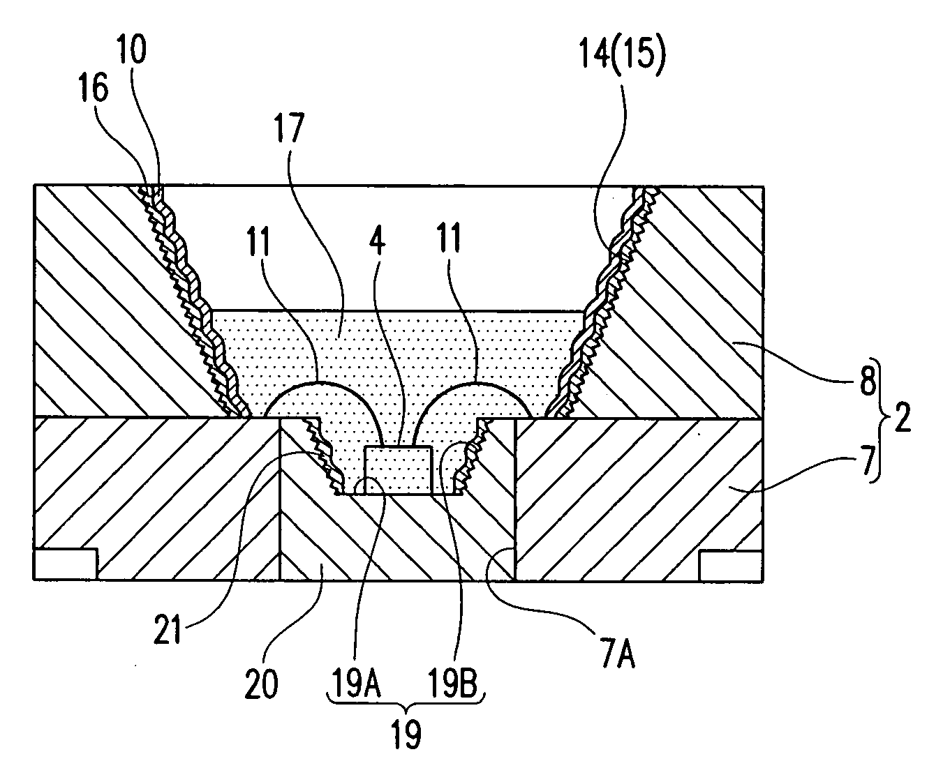
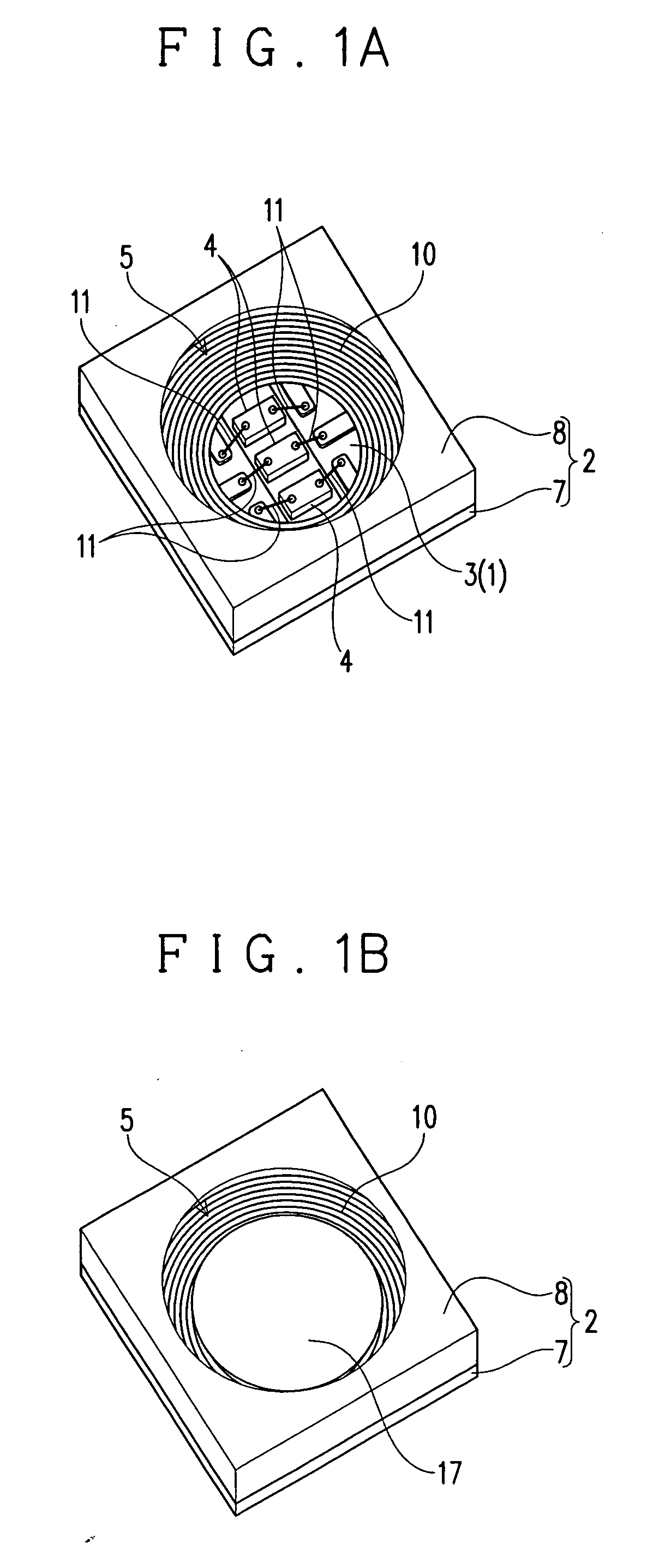
[0041]FIGS. 1A and 1B illustrate a light emitting diode as an example of a light emitting device. This light emitting diode includes a package 2 having a recessed portion 1 and three light emitting elements 4 mounted on a bottom surface 3 of the recessed portion 1. FIG. 1A illustrates the light emitting diode in a state just before it is filled with a light transmitting resin material, such as silicone resin or epoxy resin for sealing the three light emitting elements 4, and FIG. 1B illustrates the light emitting diode filled with a light transmitting material 17. Herein, illustration is made for the light emitting diode with three light emitting elements 4 disposed within the recessed portion, but it is possible to dispose one or two, or four or more light emitting elements 4 within the recessed portion. The light emitting elements 4 each have a positi...


PUM


Abstract

A light emitting device includes a package having a recessed portion defined by a bottom surface and a side surface and a light emitting element mounted on the bottom surface of the recessed portion, in which the package has fibrous fillers, and at least some of the fillers are projected outwards through the side surface and coated with a reflection film made of metal.

Description

CROSS REFERENCE TO RELATED APPLICATION[0001]This application claims priority from Japanese Patent Application No. 2006-132748, which is incorporated herein by reference.FIELD OF THE INVENTION[0002]The present invention relates to a light emitting device that includes a package having a recessed portion defined by a bottom surface and a side surface, and a light emitting element mounted on the bottom surface of the recessed portion.BACKGROUND OF THE INVENTION[0003]A light emitting diode as an example of the aforesaid light emitting device has a flat-plate like package with a light emitting element mounted thereon, and a cylindrical reflecting case as a reflector mounted on the package. The reflecting case is intended to collect light emitted from the light emitting element and spread sidewards and guide the same forward. Specifically, the reflecting case surrounds the periphery of the light emitting element so as to be able to collect light spread out from the light emitting device a...

Claims


Application Information

Patent Timeline
Patent Type & Authority Applications(United States)
IPC IPC(8): H01L33/00H01L33/32H01L33/28H01L33/46H01L33/56H01L33/60H01L33/62
CPCH01L25/0753H01L33/60H01L33/642H01L2224/48091H01L2924/00014H01L2924/00H01L2924/181H01L2924/00012
Inventor TAMAKI, HIROTOKANADA, MORITO
Owner NICHIA CORP
Why Eureka
Try Eureka