RC-Triggered Power Clamp Suppressing Negative Mode Electrostatic Discharge Stress

a technology of negative discharge and power clamp, which is applied in the direction of emergency protective circuit arrangement, emergency protective arrangement for limiting excess voltage/current, electrical equipment, etc., can solve the problems of diodes occupying valuable silicon area, not optimized for esd stress, and weak rc-triggered power clamping

a technology of negative discharge and power clamp, which is applied in the direction of emergency protective circuit arrangement, emergency protective arrangement for limiting excess voltage/current, electrical equipment, etc., can solve the problems of diodes occupying valuable silicon area, not optimized for esd stress, and weak rc-triggered power clamping

US20070285853A1Inactive Publication Date: 2007-12-13IBM CORP

Image

  • RC-Triggered Power Clamp Suppressing Negative Mode Electrostatic Discharge Stress
  • RC-Triggered Power Clamp Suppressing Negative Mode Electrostatic Discharge Stress
  • RC-Triggered Power Clamp Suppressing Negative Mode Electrostatic Discharge Stress

Examples


Embodiment Construction

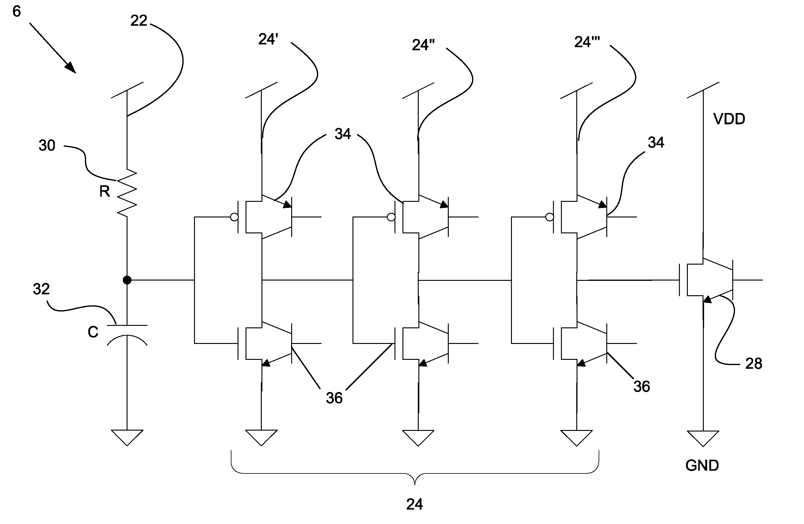
[0015]Referring now to the figures, FIG. 1 illustrates a conventional power clamp circuit 6. Power clamp circuit 6 includes an RC-delay or triggering element 22 having a resistor 30 connected in series with a capacitor 32. RC-delay element 22 is connected in series with a plurality of serialized inverters 24 connected in series with a power clamp element 28. Power for circuit 6 is typically supplied by a voltage supply referred to as VDD with ground represented by GND. During all ESD events, inverters 24 trigger on power clamp element 28 to conduct current. Power clamp circuit 6 is generally designed for positive mode ESD events. However, power clamp circuit 6 conducts poorly during negative mode ESD events.

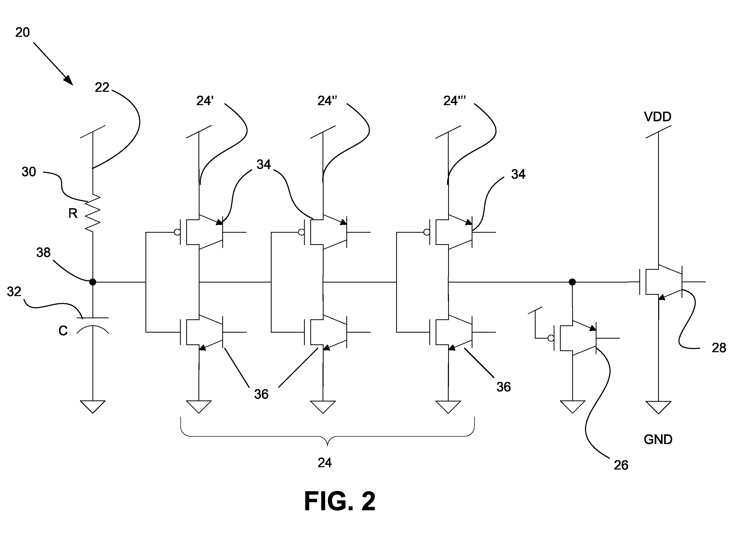
[0016]FIG. 2 illustrates one embodiment of the disclosure showing a floating-body NFET-based power clamp circuit 20 for detecting and controlling both negative and positive modes of electrostatic discharge (ESD) stress. Circuit 20 protects against all types of ESD stress events i...


PUM


Abstract

An electrostatic discharge (ESD) power clamp circuit including a RC-delay element coupled to a plurality of serialized inverter elements with a power clamp element and an ESD-triggered keeper device coupled to the plurality of inverters. During negative mode ESD events, the ESD-triggered keeper device is activated and assists the power clamp element to pull up and strongly conduct current to protect the circuit. Additionally, a method of ESD protection in a circuit is provided. The method includes coupling a RC-delay element to an input of a plurality of serialized inverter elements, coupling an output of the plurality of serialized inverters with an ESD-triggered keeper device and a power clamp element, triggering the ESD-triggered keeper device to turn on during negative ESD events and conducting current by the power clamp element with assistance of the ESD-triggered keeper device to protect the circuit as a result of negative ESD events.

Description

FIELD OF THE INVENTION[0001]The present invention generally relates to electrostatic discharge (ESD) protection circuits. In particular, the present invention is directed to a RC-triggered power clamp capable of suppressing negative mode ESD stress.BACKGROUND OF THE INVENTION:[0002]Electrostatic discharge (ESD) is a momentary and sudden electric current that flows when an excess of electric charge, stored on an electrically insulated structure, finds a path to a structure at a different electrical potential, such as ground. ESD is particularly a serious concern with microelectronic devices. The integrated circuits (IC) in these devices are made from semiconductor materials, such as silicon, and insulating materials, such as silicon dioxide, which can break down when exposed to high voltages.[0003]ESD stress occurs in two modes: positive mode ESD and negative mode ESD. Positive mode ESD occurs when there is positive ESD stress at voltage supply (VDD) and ground line is at GND (ground...

Claims


Application Information

Patent Timeline
13 Dec 2007
Publication
US20070285853A1
IPC
H02H9/00
CPC
H02H9/046
Inventors
GAUTHIER, ROBERT J.; KONTOS, DIMITRIOS K.