Method of Forming Patterns of Semiconductor Device
- Summary
- Abstract
- Description
- Claims
- Application Information
AI Technical Summary
Benefits of technology
Problems solved by technology
Method used
Image

Examples
first embodiment
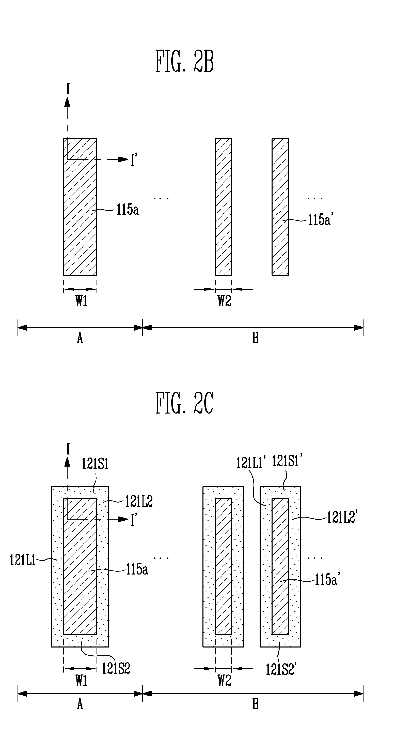
[0027]FIGS. 2A to 2J are plan views showing a method of forming patterns of a semiconductor device and FIGS. 3A to 3J are section views of the semiconductor device taken along line I-I′ shown in FIGS. 2A to 2J.
[0028]Referring to FIGS. 2A and 3A, a target etch layer 105, a hard mask layer 107, a first auxiliary layer, 129, and first photoresist patterns PR1 for forming the patterns of the semiconductor device are formed over a semiconductor substrate 101 including a first region A and a second region B (semiconductor substrate in second region B is not shown).
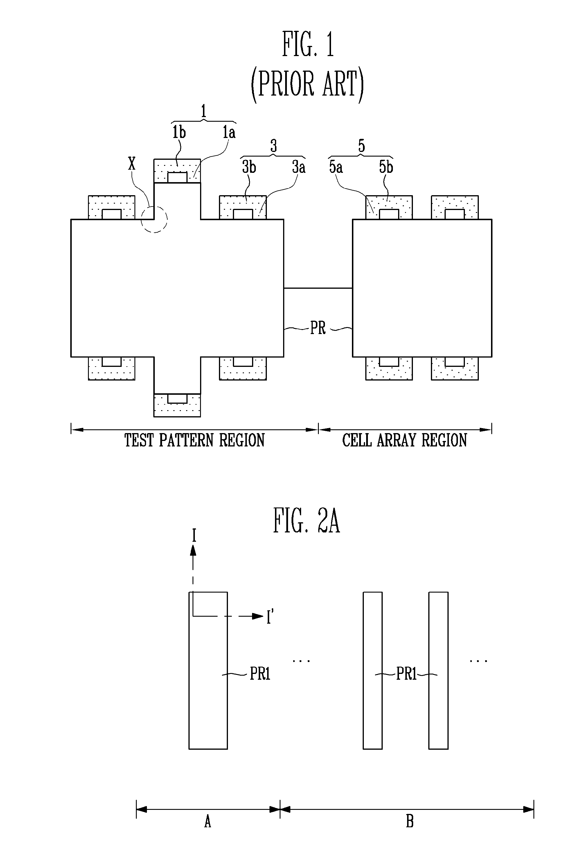
[0029]The first region A is a peri region where a test pattern and test pad units will be formed. The second region B is a cell array region where cell array patterns constituting the cell array of the semiconductor device will be formed.
[0030]The target etch layer 105 is patterned to form the target pattern, which constitutes the test pattern, the test pad units, and the cell array pattern. For example, when the cell array pat...
second embodiment
[0059]First, in the second embodiment, the first spacer is formed using the same method as that shown in FIGS. 2A and 3A, 2B and 3B, 2C and 3C, and 2D and 3D.
[0060]Referring to FIG. 4A, in the second embodiment, the first interconnection spacers are exposed. The first spacer is etched using photoresist patterns, which cover the first line spacers 121L1 and 121L2, as etch barriers. Accordingly, the first interconnection spacers are removed, but the first line spacers 121L1 and 121L2 remain in the first region A.
[0061]Referring to FIG. 4B, second sacrificial patterns 123a overlap both ends of one (for example, the first line spacer 121L2) of the first line spacers 121L1 and 121L2. A detailed description of a method of forming the second sacrificial patterns 123a is identical to that described with reference to FIGS. 2G and 3G and 2H and 3H.
[0062]The interval between the first line spacers 121L1 and 121L2 in the second embodiment is defined by the first width W1 (see FIG. 4A) described...
third embodiment
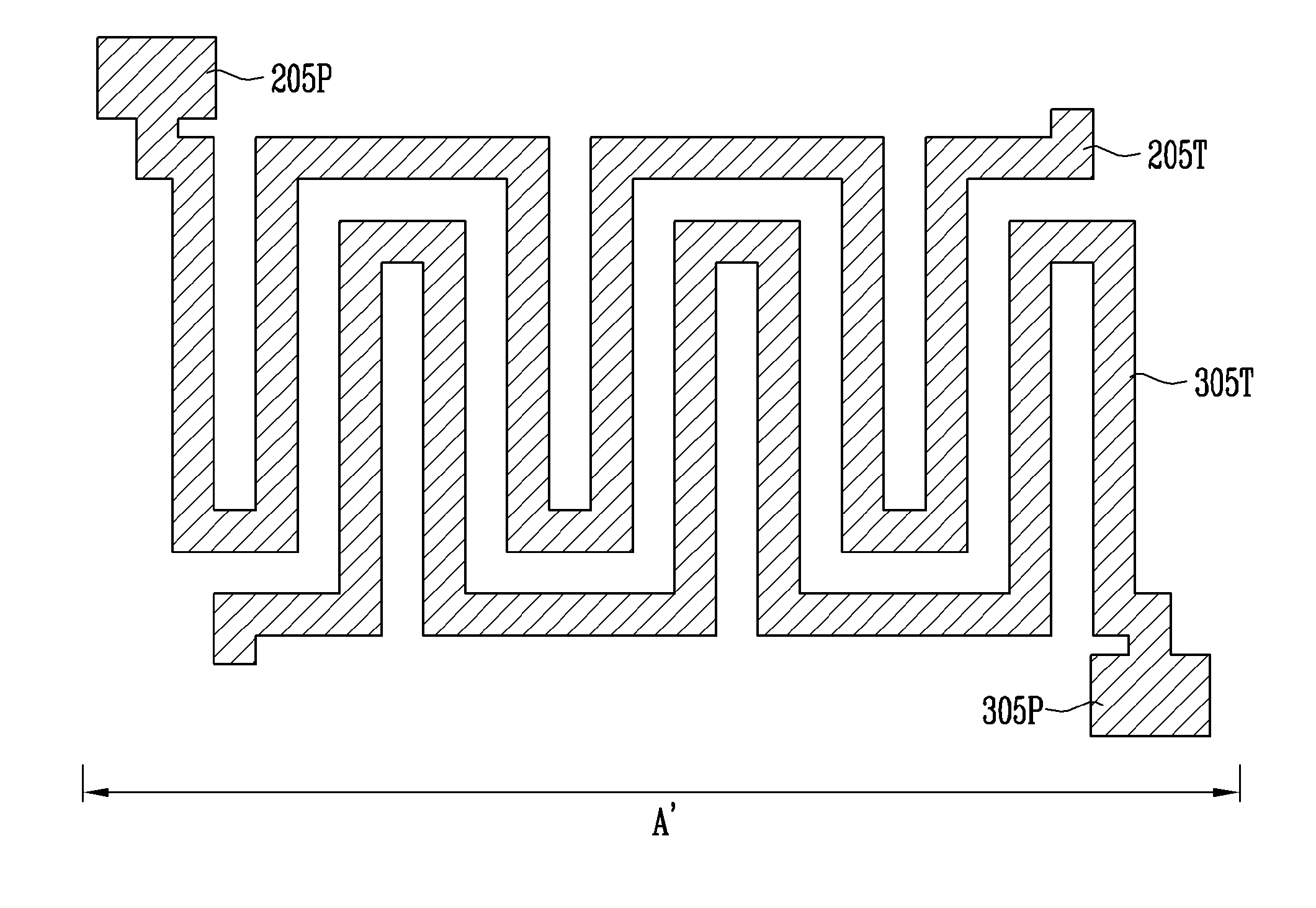
[0069]The width of the first photo pattern 251 is a factor to determine the alignment margin of an exposure mask for cutting. Accordingly, in the third embodiment, the width of the first photo pattern 251 has to be formed to secure the alignment margin of the exposure mask for cutting in a subsequent process. In more detail, the width of the first photo pattern 251 may be wider than the width of each of the first photoresist patterns (refer to PR1 of FIG. 2A) formed in the second region (refer to B of FIG. 2A). Although the width of the first photo pattern 251 may vary depending on the design rule of a semiconductor device, the width of the first photo pattern 251 is six to eight times the width of the first photoresist patterns (refer to PR1 of FIG. 2A) formed in the second region (refer to B of FIG. 2A) with DOF margin and the range of the first region A′ taken into consideration.
[0070]Each of the second photo patterns 253 may have the same density and width as the first photoresi...
PUM
 Abstract
Description
Claims
Application Information
 - Generate Ideas
- Intellectual Property
- Life Sciences
- Materials
- Tech Scout
- Unparalleled Data Quality
- Higher Quality Content
- 60% Fewer Hallucinations
Browse by: Latest US Patents, China's latest patents, Technical Efficacy Thesaurus, Application Domain, Technology Topic, Popular Technical Reports.
© 2025 PatSnap. All rights reserved.Legal|Privacy policy|Modern Slavery Act Transparency Statement|Sitemap|About US| Contact US: help@patsnap.com