
Semiconductor and Method for Manufacturing the Same

a technology of semiconductors and semiconductors, applied in the direction of semiconductor devices, electrical apparatus, transistors, etc., can solve the problems of reduced junction depth, reduced junction depth, and reduced junction depth, and achieve the effect of reducing the influence and reducing the siz

Active Publication Date: 2008-03-06
DONGBU HITEK CO LTD
View PDF23 Cites 0 Cited by
  • Summary
  • Abstract
  • Description
  • Claims
  • Application Information

AI Technical Summary

Benefits of technology

[0009]Embodiments of the present invention provide a manner for reducing the influence caused by means of a lateral diffusion of a deep source / drain. An embodiment addresses the effect on the performance of a device as a sidespacer wall width of a CMOS FET device; in particular, a PMOS reduces in size. According to an embodiment, a method is provided for securing a margin of a sidewall spacer forming process.
[0010]Embodiments of the present invention provide a semiconductor device and a method for manufacturing thereof capable of minimizing the degradation in performance of a PMOS device due to a lateral diffusion and securing a process margin of a sidespacer wall width by applying indium and BF2 relatively heavier than boron, unlike a process forming a deep source / drain by applying only boron in an existing PMOS device.

Problems solved by technology

In particular, in the case of a PMOS, since a deep source / drain ion implant process typically uses light boron, it is considered to be more fragile from the influence of the lateral diffusion from the deep source / drain, as compared to an NMOS.
However, the junction depth is reduced to the size of about 30 nm or less, and any disadvantages due to the reduced junction depth may occur.

Method used


Image

  • Semiconductor and Method for Manufacturing the Same
  • Semiconductor and Method for Manufacturing the Same
  • Semiconductor and Method for Manufacturing the Same

Examples


Embodiment Construction

[0015]Hereinafter, a semiconductor device and a method for manufacturing the same according to an embodiment of the present invention will be described with reference to the accompanying drawings.

[0016]In the description of embodiments, it will be understood that when a layer (or film) is referred to as being ‘on’ another layer or substrate, it can be directly on another layer or substrate, or intervening layers may also be present. Further, it will be understood that when a layer is referred to as being ‘under’ another layer, it can be directly under another layer, and one or more intervening layers may also be present. In addition, it will also be understood that when a layer is referred to as being ‘between’ two layers, it can be the only layer between the two layers, or one or more intervening layers may also be present.

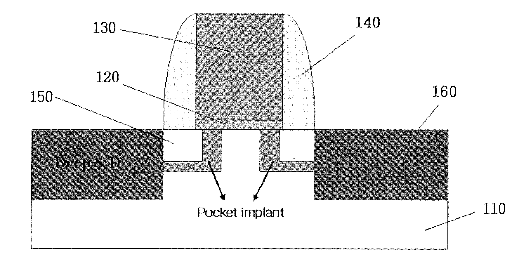
[0017]FIG. 1 is a cross-sectional view of a semiconductor device according to a first embodiment.

[0018]Referring to FIG. 1, a substrate 110 can be provided with ...


PUM


Abstract

A semiconductor device and a method of fabricating same are provided. According to an embodiment, a gate insulating layer and a gate are sequentially formed on a substrate, and a pocket ion implant region is formed at sides and below a portion of the gate at a predetermined depth in the substrate. An LDD ion implant region can be formed between the pocket ion implant region and the surface of the substrate. A spacer is formed on sides of the gate, and a deep source / drain region is formed by ion-implanting BF2 within the substrate at sides of the spacer.

Description

CROSS-REFERENCE TO RELATED APPLICATION[0001]The present application claims the benefit under 35 U.S.C. §119 of Korean Patent Application No. 10-2006-0083916, filed Aug. 31, 2006, which is hereby incorporated by reference in its entirety.BACKGROUND[0002]Currently, in a process for manufacturing a CMOS FET device, as the size of the device becomes smaller, a sidespacer wall width applied as a hard mask for a deep source / drain ion implant also becomes smaller.[0003]Thereby, the influence due to a lateral diffusion of the deep source / drain dopant is reflected in the electrical characteristics of the device (reduction in Vth and increase in leakage current).[0004]In particular, in the case of a PMOS, since a deep source / drain ion implant process typically uses light boron, it is considered to be more fragile from the influence of the lateral diffusion from the deep source / drain, as compared to an NMOS.[0005]Meanwhile, an attempt to reduce the channeling in a vertical or a depth direction...

Claims


Application Information

Patent Timeline
IPC IPC(8): H01L29/94H01L21/336
CPCH01L21/26586H01L29/7833H01L29/6653H01L29/66492H01L29/6659
Inventor JEON, HACNG LEEM
Owner DONGBU HITEK CO LTD
Features
  • Generate Ideas
  • Intellectual Property
  • Life Sciences
  • Materials
  • Tech Scout
  • Unparalleled Data Quality
  • Higher Quality Content
  • 60% Fewer Hallucinations
Learn More