

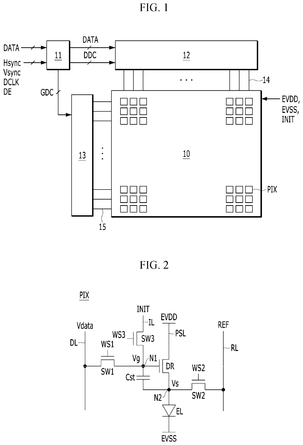
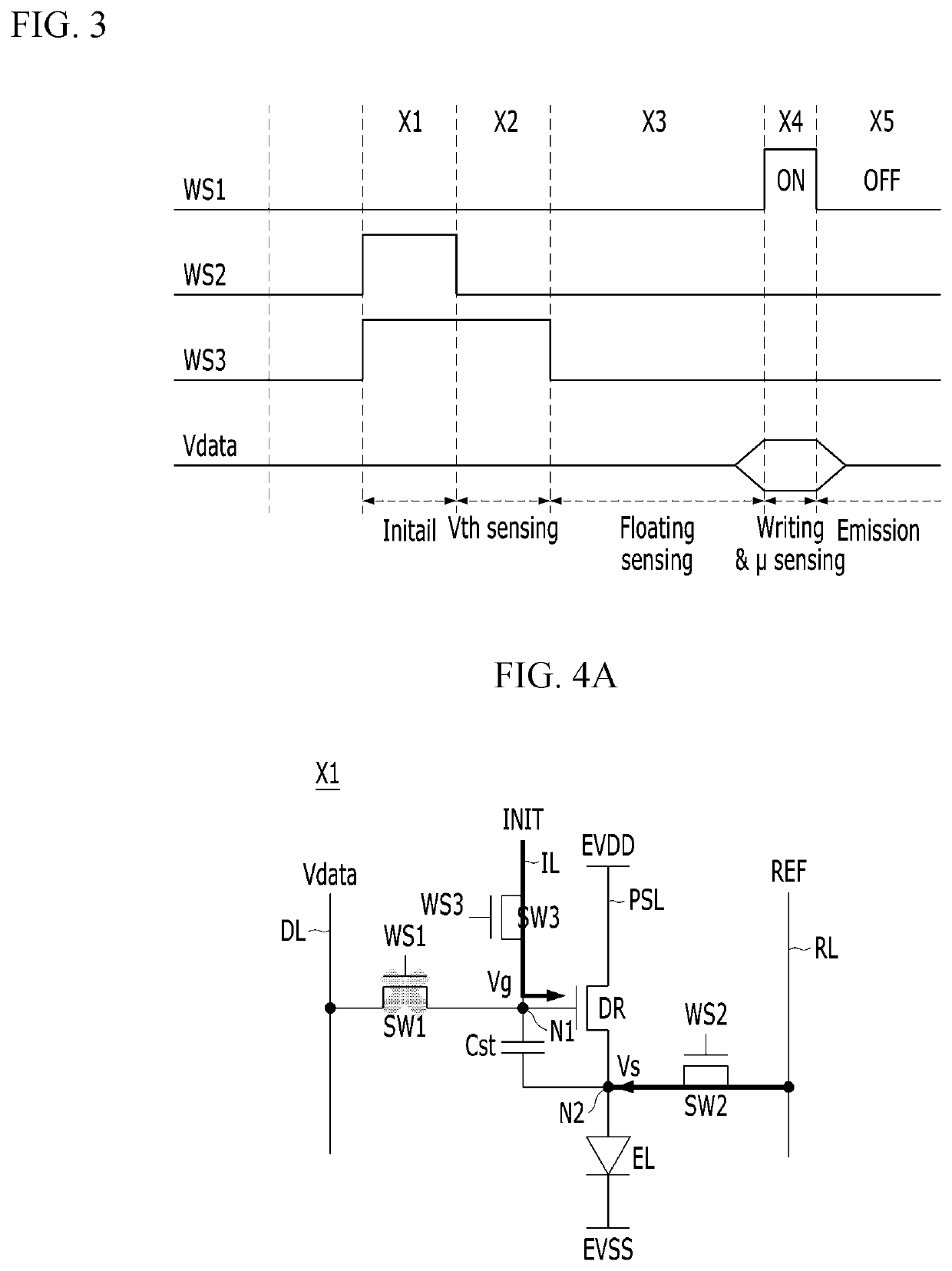
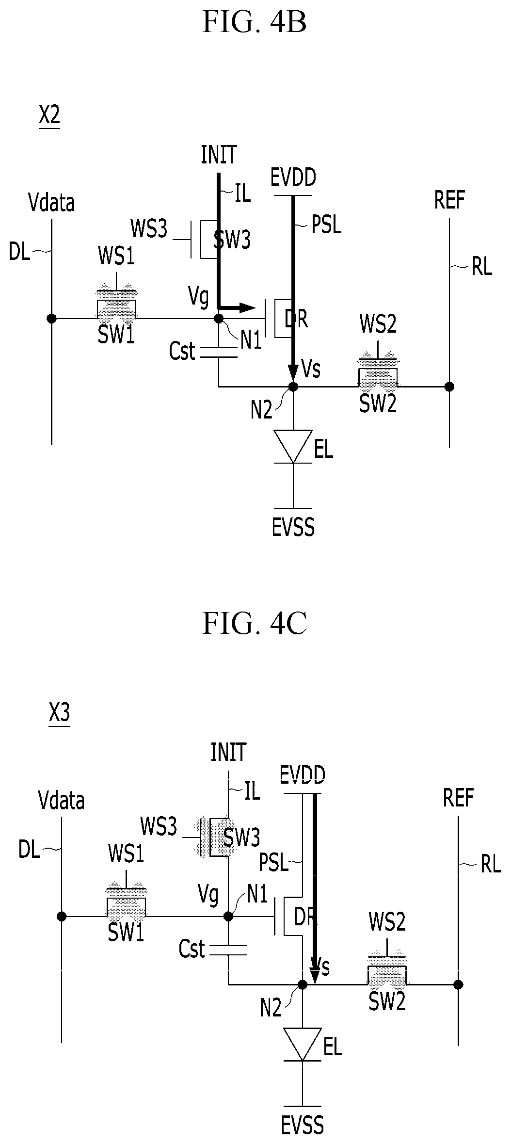
Electroluminescent display device
a technology of display device and electroluminescent light, which is applied in the direction of static indicating device, instruments, etc., can solve the problems of limited panel design and serious problems in the related art, and achieve the effect of reducing manufacturing cost, ensuring processing margin, and reducing manufacturing costs
- Summary
- Abstract
- Description
- Claims
- Application Information
AI Technical Summary
Benefits of technology
Problems solved by technology
Method used
Image

Examples
first embodiment
[0061]FIG. 5 to FIG. 7 are diagrams showing configurations of connections between two pixels and signal lines (including data lines and gate lines) according to a first embodiment of the present disclosure.
[0062]Referring to FIG. 5 and FIG. 6, two pixels P1 and P2 according to the first embodiment are contiguously disposed in the horizontal direction having a data line DL interposed therebetween and are driven in a time division manner while sharing the data line DL for DRD internal compensation.
[0063]The first pixel P1 may include a first light-emitting element EL1 having a first color, a first driving transistor DR1 that drives the first light-emitting element EL1, a first group of switching transistors SW11, SW12, and SW13 connected to the first driving transistor DR1, and a first storage capacitor Cst1 and operate in the method as described with reference to FIG. 3 to FIG. 4E.
[0064]The second pixel P2 may include a second light-emitting element EL2 having a second color, a secon...
second embodiment
[0099]FIG. 14 to FIG. 16 are diagrams showing configurations of connections between two pixels and signal lines according to a second embodiment of the present disclosure.
[0100]Referring to FIG. 14 and FIG. 15, two pixels P1 and P2 according to the second embodiment are contiguously disposed in the horizontal direction having a data line DL interposed therebetween and share the data line DL to be driven in a time division manner for DRD internal compensation.
[0101]The first pixel P1 may include a first light-emitting element EL1 having a first color, a first driving transistor DR1 that drives the first light-emitting element EL1, a first group of switching transistors SW11, SW12, and SW13 connected to the first driving transistor DR1, and a first storage capacitor Cst1 and may operate through a method similar to that described above with reference to FIG. 3 to FIG. 4E.
[0102]The second pixel P2 may include a second light-emitting element EL2 having a second color, a second driving tr...
third embodiment
[0138]FIG. 22 is a diagram showing a configuration of connections between four pixels distributed and disposed in each of three pixel lines and signal lines according to a third embodiment of the present disclosure.
[0139]Referring to FIG. 22, in the third embodiment, the number of gate lines necessary for DRD internal compensation is reduced through a configuration in which four pixels P1 to P4 that neighbor each other in the horizontal and vertical directions are connected to five gate lines.
[0140]The four pixels P1 to P4 include a first pixel P1, a second pixel P2, a third pixel P3, and a fourth pixel P4 that share the same data line. The first pixel P1 and the fourth pixel P4 may include a red light emitting element R (EL), and the second pixel P2 and the third pixel P3 may include a white light emitting element W (EL).
[0141]The first pixel P1 and the second pixel P2 are contiguously disposed in the horizontal direction having the data line interposed therebetween and additionall...
PUM
 Abstract
Description
Claims
Application Information