
Method for manufacturing a magnetic memory device, and a magnetic memory device

a technology of magnetic memory and manufacturing method, which is applied in the direction of digital storage, semiconductor devices, instruments, etc., to achieve the effect of efficient introduction, efficient introduction of memory elements, and reduction of the number of steps

Inactive Publication Date: 2006-05-04
SONY CORP
View PDF3 Cites 1 Cited by
  • Summary
  • Abstract
  • Description
  • Claims
  • Application Information

AI Technical Summary

Benefits of technology

[0034] The first method for manufacturing a magnetic memory device has a step of removing the insulating film on a side portion of the second wiring to expose the second wiring, and a step of forming a soft magnetic material layer selectively only on a surface of the second wiring. Therefore, the sidewall of the second wiring and the upper surface of the second wiring are covered with the soft magnetic material layer selectively formed, so that a current magnetic field generated in the second wiring can be efficiently introduced to the memory element. In addition, the soft magnetic material layer is selectively formed, and hence a conventional lithography technique, etching technique or the like is not needed, and the layer can be formed by an electroless plating process, thus making it possible to reduce the number of the steps. Further, no etchback by dry etching is conducted for the soft magnetic material layer, and therefore stability and margin of the process can be secured. In addition, there is no need to consider alignment tolerance of the mask for lithography, making shrinking possible. Further, the soft magnetic material layer is not formed directly on the insulating film, and hence the insulating film suffers no contamination due to the soft magnetic material layer.
[0043] Further, in the method of the present invention, a step of forming a soft magnetic material layer on the bottom of a wiring trench is not required, and therefore no particles are generated by etching for removing the soft magnetic material layer on the bottom of the wiring trench, so that the yield of the magnetic memory device can be improved.

Problems solved by technology

Further, no etchback by dry etching is conducted for the soft magnetic material layer, and therefore stability and margin of the process can be secured.

Method used


Image

  • Method for manufacturing a magnetic memory device, and a magnetic memory device
  • Method for manufacturing a magnetic memory device, and a magnetic memory device
  • Method for manufacturing a magnetic memory device, and a magnetic memory device

Examples


first embodiment

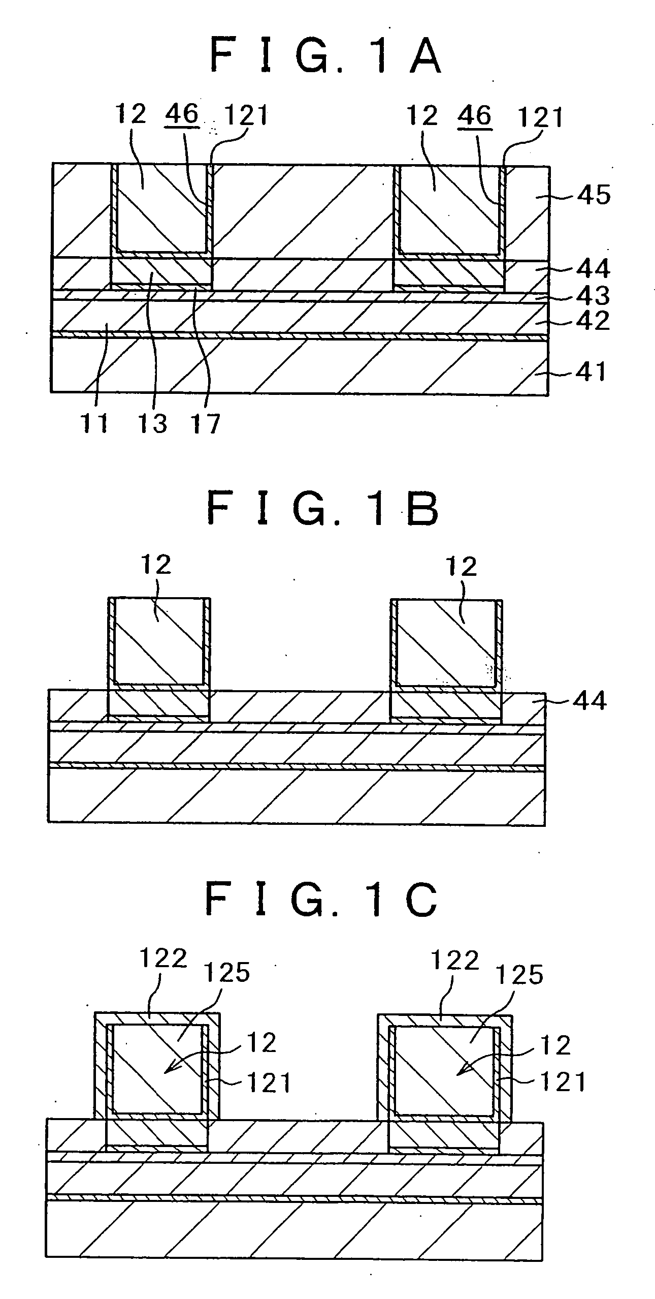
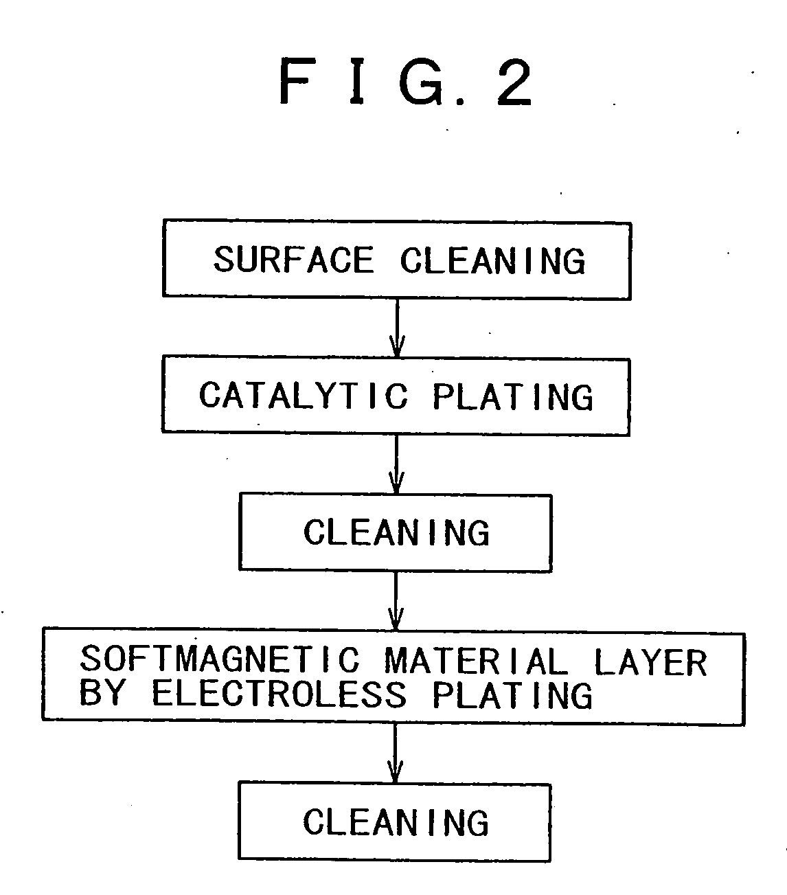
[0054] The method for manufacturing a magnetic memory device and the magnetic memory device according to the present invention will be described with reference to the diagrammatic cross-sectional views of steps of FIGS. 1A to 1C. The cross-sectional views for the embodiments below are those taken along the line in the width direction of a bit line, namely, cross-sectional views taken along the line in the direction of a word line.

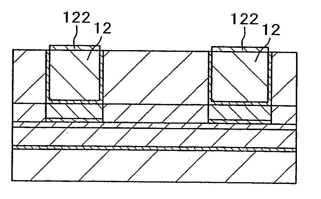
[0055] As shown in FIG. 1A, an element for selection (not shown), a sense line (not shown), and the like are formed on a substrate (not shown), and a first insulating film 41 is formed so as to cover them. On the first insulating film 41 is formed a second insulating film 42 in which a word line and the like are formed, and in the second insulating film 42 are formed a word line (first wiring) 11 having a trench wiring structure, an electrode (not shown) connected to the element for selection (not shown), and the like. On the second insulating film 42, a me...

second embodiment

[0084] Next, the method for manufacturing a magnetic memory device and the magnetic memory device according to the present invention will be described with reference to the diagrammatic cross-sectional views of steps of FIGS. 4A to 4D.

[0085] The second embodiment is a method having an effect to further improve the selectivity for the soft magnetic material layer in the first embodiment. A difference between the second embodiment and the first embodiment resides in that, after removal of the fifth insulating film, a process for removing the barrier metal layer on the bit line is introduced. By removing the barrier metal layer, the entire surface of the bit line is comprised of copper, facilitating selective growth of the soft magnetic material layer. This attributes to deposition of palladium by catalytic plating. A high melting point metal is used in the barrier metal layer, and hence it is not easy to deposit a catalyst metal layer on the barrier metal layer. On the other hand, the...

third embodiment

[0091] Next, the method for manufacturing a magnetic memory device and the magnetic memory device according to the present invention will be described with reference to the diagrammatic cross-sectional views of steps FIGS. 5A to 5E.

[0092] For achieving selective complete coverage for the bit line by electroless plating in the first and second embodiments, in the third embodiment, a so-called lift-off method is used in which a mask is formed on a portion on which a soft magnetic material layer is not deposited and a soft magnetic material layer is deposited by selective electroless plating, followed by removal of the mask. The third embodiment is described below.

[0093] As shown in FIG. 5A, the bit line 12 having a trench wiring structure is formed in the fifth insulating film 45 in the same manner as that described above with reference to FIG. 1A.

[0094] Then, as shown in FIG. 5B, the fifth insulating film 45 {see FIG. 5A} is removed in the same manner as that described above with r...


PUM


Abstract

In bit line cladding structure formation, stability and margin of the process are secured and further shrinking is achieved, and the magnetic memory device is improved in speed, reliability and yield. Method for manufacturing a magnetic memory device, comprising the steps of: forming a word line; forming a magnetoresistance effect memory element comprising a tunnel insulating layer disposed between a ferromagnetic material and being electrically insulated from the word line; forming an insulating film for covering the memory element; and forming a bit line so that it is buried in the insulating film wherein the bit line is electrically connected to the memory element and spatially crosses the word line through the memory element disposed therebetween, wherein the method has steps of removing the insulating film on the bit line side to expose the bit line and forming a soft magnetic material layer selectively only on the bit line surface.

Description

CROSS REFERENCE TO RELATED APPLICATION [0001] This application claims priority from Japanese Priority Document No. 2003-066081, filed on Mar. 12, 2003 with the Japanese Patent Office, which document is hereby incorporated by reference. BACKGROUND OF THE INVENTION [0002] 1. Field of the Invention [0003] The present invention relates to a method for manufacturing a magnetic memory device and a magnetic memory device. More particularly, the present invention is concerned with a method for manufacturing a nonvolatile magnetic memory device and a magnetic memory device which stores information by utilizing a change of the resistance value caused by changing of the spin direction of a ferromagnetic material to be parallel or non-parallel. [0004] 2. Description of Related Art [0005] As information communication devices, especially small devices for personal use, such as mobile terminals, are rapidly spreading, there are demands for devices constituting such electronic devices, such as a me...

Claims


Application Information

Patent Timeline
IPC IPC(8): H01L21/8232H01L27/105G11C11/16H01L21/8246H01L27/115H01L27/22
CPCG11C11/16H01L27/222H01L43/12H01L21/76885H01L21/76852H01L21/76865H10B61/00H10N50/01
Inventor HORIKOSHI, HIROSHI
Owner SONY CORP
Features
  • Generate Ideas
  • Intellectual Property
  • Life Sciences
  • Materials
  • Tech Scout
  • Unparalleled Data Quality
  • Higher Quality Content
  • 60% Fewer Hallucinations
Learn More