
Method for manufacturing a nonvolatile memory device

a memory device and non-volatile technology, applied in the direction of semiconductor devices, basic electric elements, electrical appliances, etc., can solve the problems of inability to manufacture mask patterns with fine size, inability to meet the requirements of input data,

Inactive Publication Date: 2010-10-26
SK HYNIX INC
View PDF10 Cites 1 Cited by
  • Summary
  • Abstract
  • Description
  • Claims
  • Application Information

AI Technical Summary

Benefits of technology

The present invention provides a method for manufacturing a nonvolatile memory device with finer contact holes. The method involves forming an etch mask pattern with an opening wider at the upper end than the lower end, and then using this pattern to define contact holes in a dielectric layer. The contact holes are defined by removing portions of the dielectric layer using the etch mask pattern. The etch mask pattern is formed by patterning an etch mask layer with multiple layers and then using slope etching to remove the byproduct produced during the etching process. The method also involves patterning a passivation layer and a BARC layer using an inductively coupled plasma etching process. The contact holes are defined using a CF4 gas etchant gas. The method provides a more efficient way to manufacture nonvolatile memory devices with finer contact holes.

Problems solved by technology

In volatile memory devices, even though the input and output of data can be quickly implemented as in a dynamic random access memory (DRAM) and a static random access memory (SRAM), if a power supply fails or is turned off, input data is lost.
However, due to a limit in the precision of exposure equipment, limitations necessarily exist in forming the mask pattern to have a fine size.
Therefore, difficulties are caused in the process for finely defining the contact holes in the dielectric layer.

Method used


Image

  • Method for manufacturing a nonvolatile memory device
  • Method for manufacturing a nonvolatile memory device
  • Method for manufacturing a nonvolatile memory device

Examples


Embodiment Construction

[0014]Reference will now be made in detail to a specific embodiment of the invention, an example of which is illustrated in the attached drawings.

[0015]It is to be noted that the present invention must not be construed as being limited to the following embodiment and can be realized in a variety of ways, and the scope of the present invention must not be limitedly understood by the following embodiment. Also, those persons who have ordinary knowledge in the art will appreciate that various embodiments are possible without departing from the technical concept of the present invention. The embodiment is provided to make the disclosure of the present invention complete and to allow those persons having ordinary knowledge in the art to better understand the scope of the present invention. The scope of the present invention must be understood by the accompanying claims.

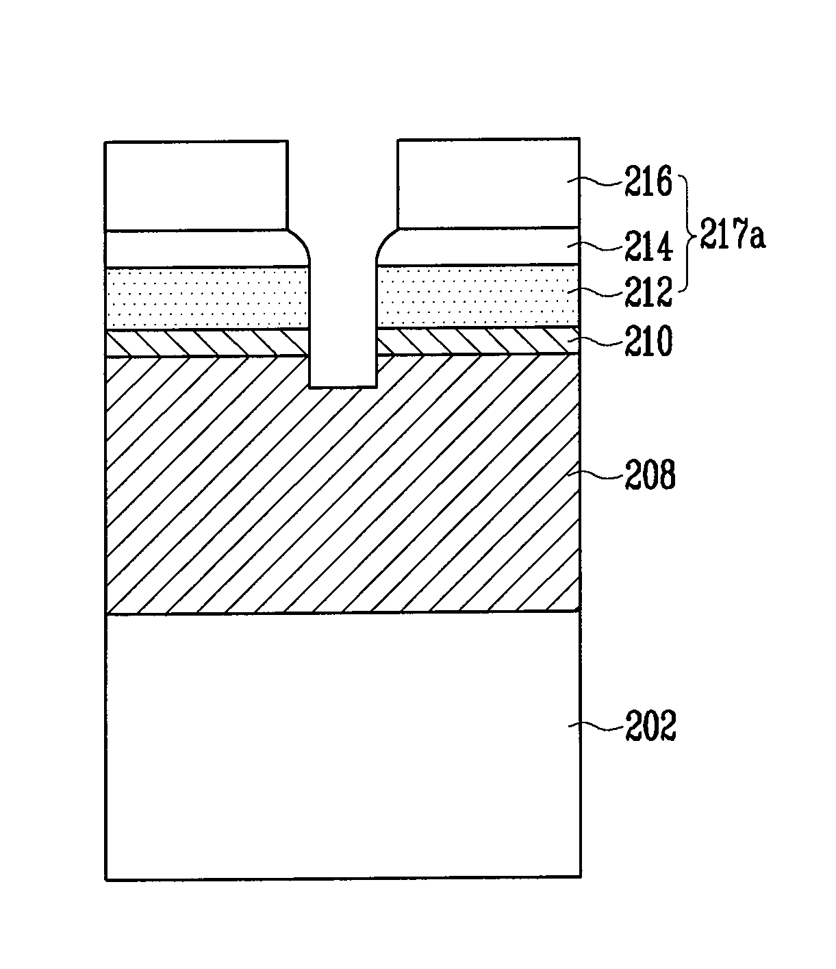
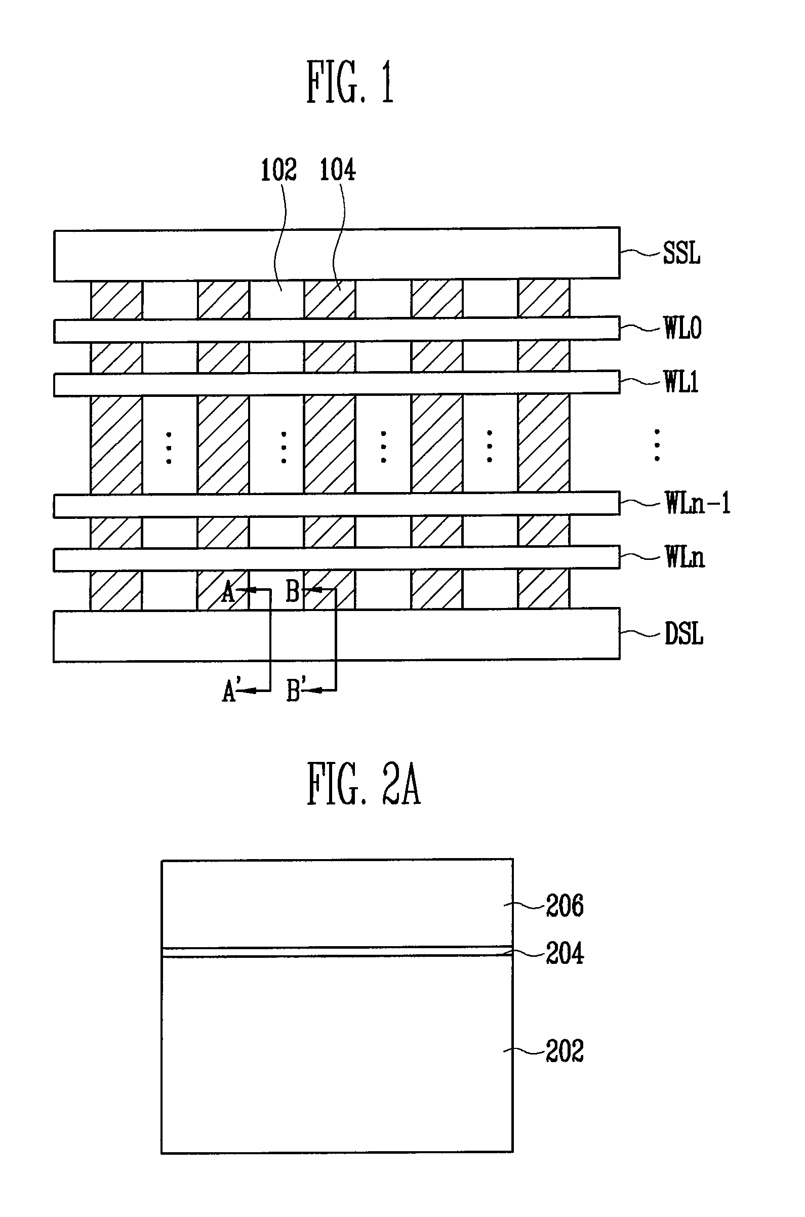
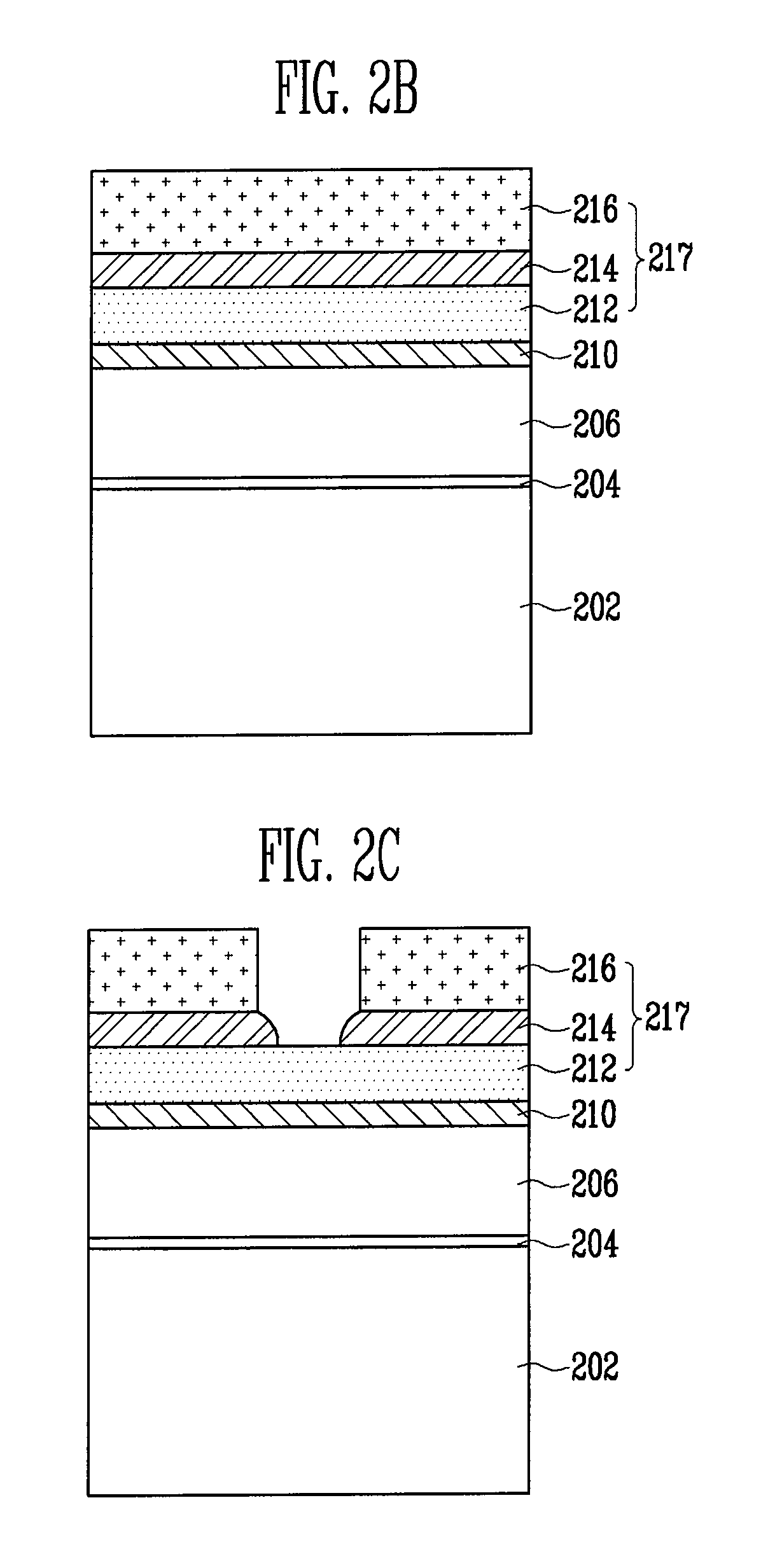
[0016]FIG. 1 is a layout diagram of a nonvolatile memory device illustrating a method for manufacturing a nonvolatile me...


PUM


Abstract

In a method for manufacturing a nonvolatile memory device, an etch mask layer formed on a dielectric layer to define contact holes in the dielectric layer is slope-etched to form an etch mask pattern having an opening wider at the upper end thereof than the lower end thereof. Thus, the contact holes are defined in the dielectric layer to have a finer size than the upper end of the opening of the etch mask pattern. The method for manufacturing a nonvolatile memory device includes forming an etch mask pattern on a dielectric layer such that a width of a lower end of each opening defined in the etch mask pattern is less than a width of an upper end thereof; and defining contact holes by removing portions of the dielectric layer using the etch mask pattern.

Description

CROSS-REFERENCE TO RELATED APPLICATIONS[0001]This application claims priority from Korean Patent Application No. 10-2008-0008498, filed on Jan. 28, 2008, the contents of which are incorporated herein by reference in its entirety.BACKGROUND OF THE INVENTION[0002]The present invention relates to a method for manufacturing a nonvolatile memory device, and more particularly, to a method for manufacturing a nonvolatile memory device which is used to manufacture a NAND flash memory device.[0003]In general, semiconductor memory devices are categorized into volatile memory devices and nonvolatile memory devices. In volatile memory devices, even though the input and output of data can be quickly implemented as in a dynamic random access memory (DRAM) and a static random access memory (SRAM), if a power supply fails or is turned off, input data is lost. In nonvolatile memory devices, even when a power supply fails or is turned off, stored data is retained continuously.[0004]A flash memory dev...

Claims


Application Information

Patent Timeline
Patent Type & Authority Patents(United States)
IPC IPC(8): H01L21/336H01L21/8234H10B69/00
CPCH01L27/115H01L27/11521H10B69/00H10B41/30H01L21/3213H01L21/76224
Inventor LEE, IN NO
Owner SK HYNIX INC
Features
  • Generate Ideas
  • Intellectual Property
  • Life Sciences
  • Materials
  • Tech Scout
  • Unparalleled Data Quality
  • Higher Quality Content
  • 60% Fewer Hallucinations
Learn More