Method of fabricating a recess channel array transistor using a mask layer with a high etch selectivity with respect to a silicon substrate

Active Publication Date: 2005-06-23
SAMSUNG ELECTRONICS CO LTD
View PDF11 Cites 55 Cited by
  • Summary
  • Abstract
  • Description
  • Claims
  • Application Information

AI Technical Summary

Benefits of technology

[0026] When forming the recess channel trench, the etch selectivity of the mask layer pattern with respect to the silicon substrate may be about 3:1. When the recess channel trench is formed, a portion of the mask layer pattern remains because of the high etch selectivity with respect to the si

Problems solved by technology

Increased integration densities and decreased design rules of integrated semiconductor devices place challenges on the stable operation of transistors.
Such punchthrough is regarded as a major cause of malfunctions in the transistor device.
Secondly, over-etching is performed.
The conventional method of fabricating the recess channel array transistor including the processing step shown in FIG. 3 is disadvantageous in that the buffer insulating layer 106 cannot be effec

Method used


Image

  • Method of fabricating a recess channel array transistor using a mask layer with a high etch selectivity with respect to a silicon substrate
  • Method of fabricating a recess channel array transistor using a mask layer with a high etch selectivity with respect to a silicon substrate
  • Method of fabricating a recess channel array transistor using a mask layer with a high etch selectivity with respect to a silicon substrate

Examples


Embodiment Construction

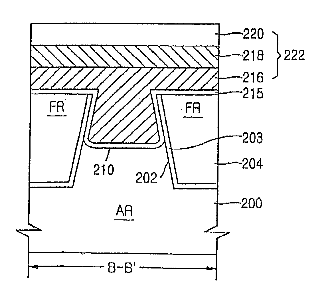
[0037] The invention will now be described more fully with reference to the accompanying drawings. The invention may, however, be embodied in many different forms and should not be construed as being limited to the embodiments set forth herein; rather these embodiments are provided so that this disclosure will be thorough and complete, and will fully convey the concept of the invention to those skilled in the art. In the drawings, the thicknesses of layers and regions are exaggerated for clarity.

[0038]FIG. 9 illustrates a layout of a mask layer pattern used to a method of fabricating a recess channel array transistor according to an aspect of the present invention.

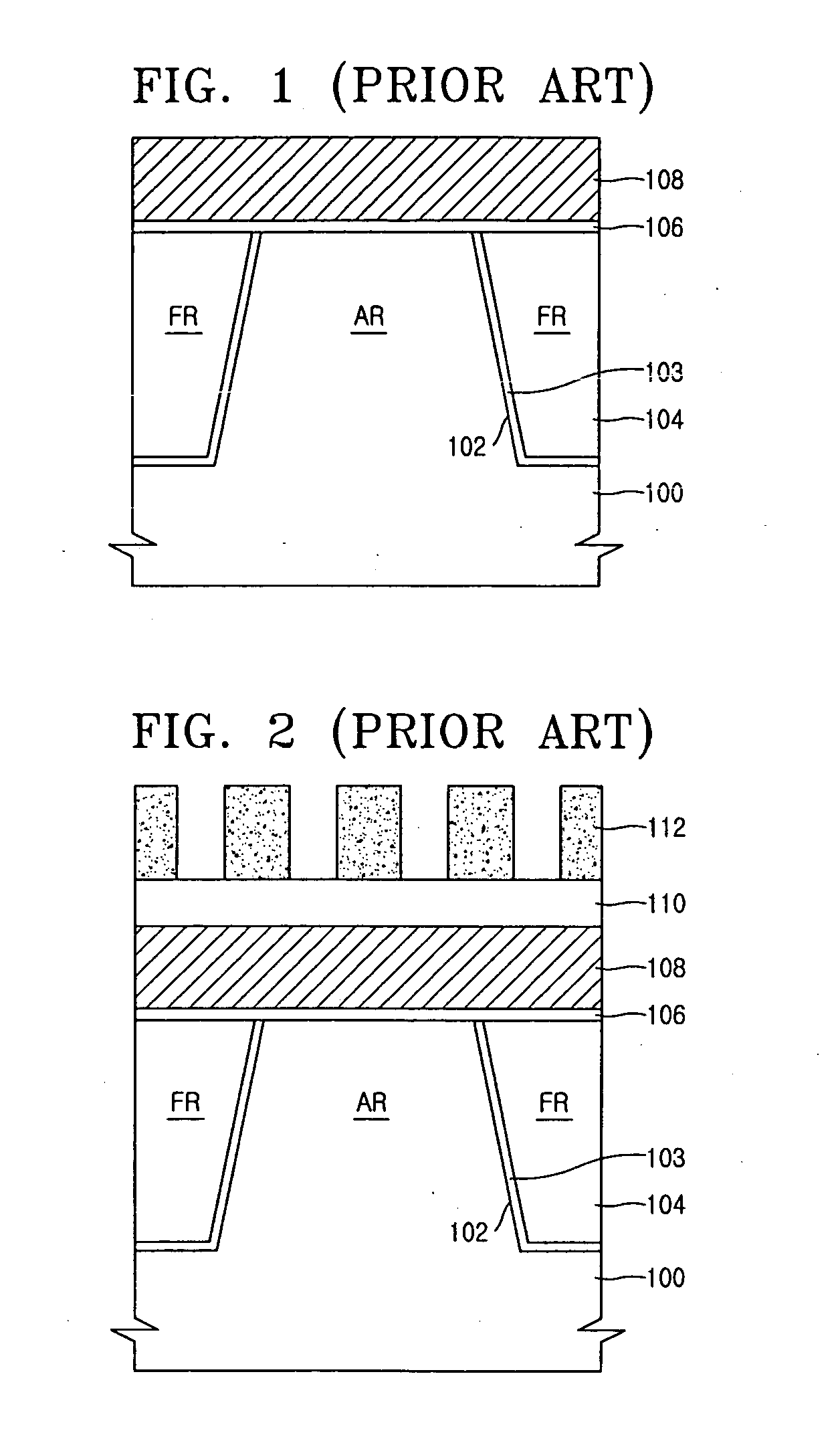
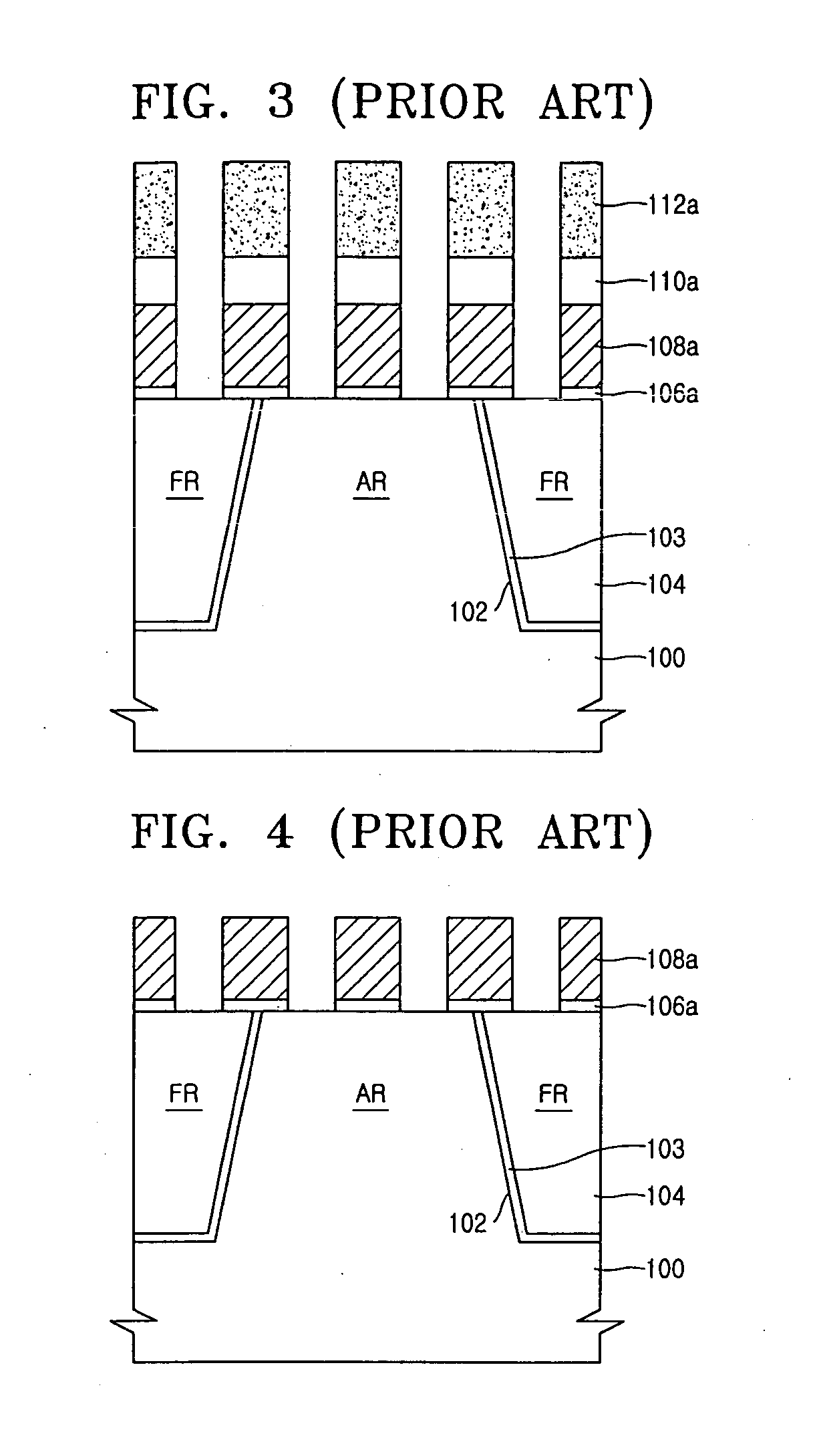
[0039] Referring to FIG. 9, an active region AR for forming a recess channel array transistor is defined on a silicon substrate 200 (FIG. 10). A region outside the active region AR is a field region FR, formed with a trench insulating layer. A mask layer pattern MP formed in a straight line pattern crosses the active reg...


PUM


Abstract

A method of fabricating a recess channel array transistor. Using a mask layer pattern having a high etch selectivity with respect to a silicon substrate, the silicon substrate and an isolation insulating layer are etched to form a recess channel trench. After forming a gate insulating layer and a recess gate stack on the recess channel trench, a source and a drain are formed in the silicon substrate adjacent to both sidewalls of the recess gate stack, thereby completing the recess channel array transistor. Because the mask layer pattern having the high etch selectivity with respect to the silicon substrate is used, a depth of the recess channel trench is easily controlled while good etching uniformity of the silicon substrate is obtained.

Description

BACKGROUND OF THE INVENTION [0001] This application claims the priority of Korean Patent Application No. 2003-93682, filed on Dec. 19, 2003, in the Korean Intellectual Property Office, the disclosure of which is incorporated herein in its entirety by reference. [0002] 1. Field of the Invention [0003] The present invention relates to a method of fabricating a transistor semiconductor device, and more particularly to a method of fabricating a recess channel array transistor. [0004] 2. Description of the Related Art [0005] Increased integration densities and decreased design rules of integrated semiconductor devices place challenges on the stable operation of transistors. For example, a decreased design rule of an integrated circuit device results in a decrease of a gate width, so that a channel of a transistor is significantly shortened. Accordingly, a so-called short channel effect frequently occurs. [0006] A short channel induces punchthrough between a source and a drain of a transi...

Claims


Application Information

Patent Timeline
IPC IPC(8): H01L21/3065H01L21/28H01L21/336H01L21/76H01L21/8234H01L29/423H01L29/78
CPCH01L21/28061H01L21/28114H01L29/66621H01L29/42376H01L21/823487H01L21/18
Inventor CHO, YOUNG-SUNAHN, TAE-HYUKJEON, JEONG-SICHONG, JUN-SIKKIM, JI-HONGPARK, HONG-MI
Owner SAMSUNG ELECTRONICS CO LTD
Why Eureka
Try Eureka