All quantum dot based optoelectronic device

Active Publication Date: 2018-09-06
TOYOTA JIDOSHA KK +1
View PDF6 Cites 14 Cited by
  • Summary
  • Abstract
  • Description
  • Claims
  • Application Information

AI Technical Summary

Benefits of technology

[0046]In this way, the same procedure may be employed, in order to prepare all quantum dots of the electron transport layer, the active layer, and the hole tr

Problems solved by technology

However, the performance of the abovementioned all-inorganic devices has been seriously degraded thus far by quenching of the active CQD by the metal oxide layer, and by imbalanced charge

Method used


Image

  • All quantum dot based optoelectronic device
  • All quantum dot based optoelectronic device
  • All quantum dot based optoelectronic device

Examples


Example

[0061]Reference will now be made in detail to exemplary embodiments of the disclosure, examples of which are illustrated in the accompanying drawings. Wherever possible, the same reference numbers will be used throughout the drawings to refer to the same or like parts.

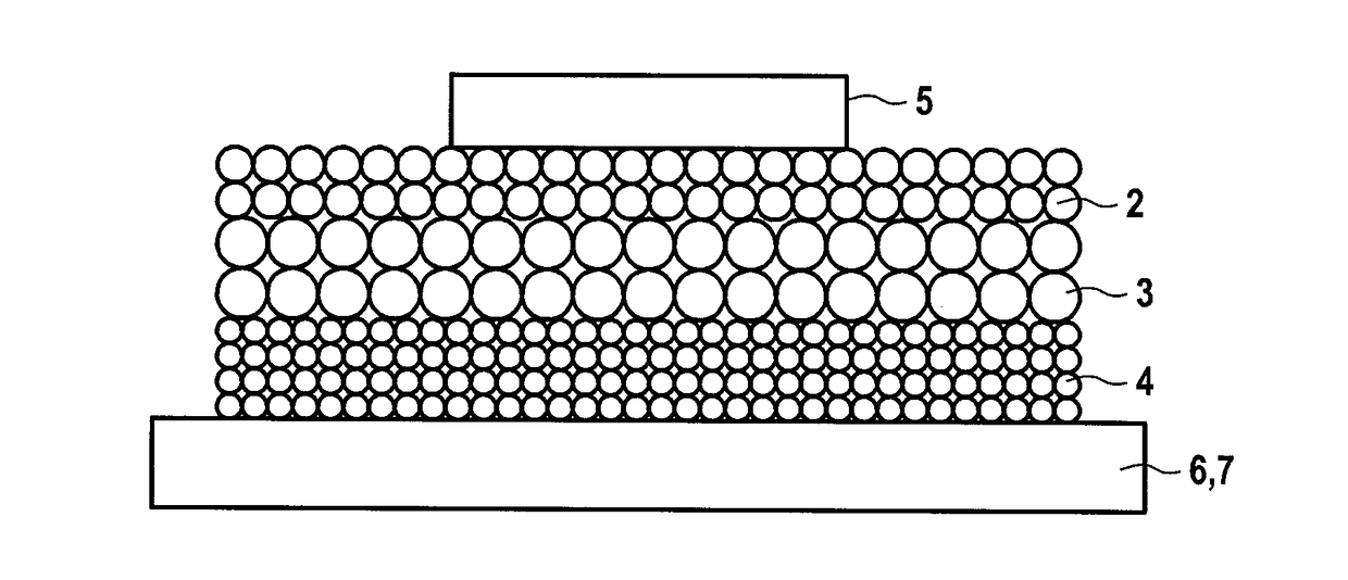
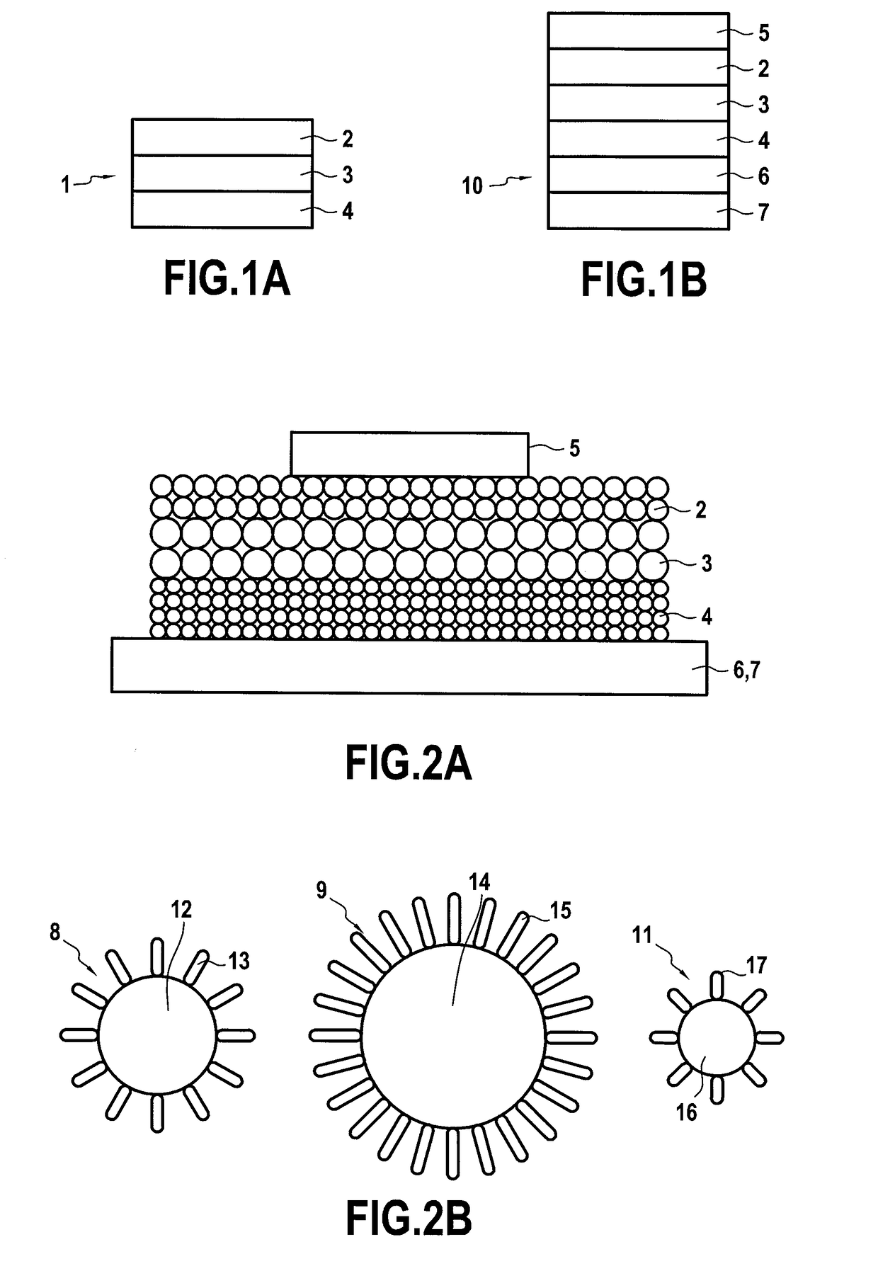
[0062]FIG. 1A shows a schematic representation of an exemplary LED (optoelectronic device) 1 according to the present disclosure. The LED comprises an electron transport layer (ETL) 2, an active layer 3 and a hole transport layer (HTL) 4. The active layer is arranged between the electron transport layer (ETL) 2 and the hole transport layer (HTL) 4. The electron transport layer (ETL) 2 and the hole transport layer (HTL) 4 comprise quantum dots, preferably they consist of quantum dots. Also the active layer 3 preferably comprises quantum dots, more preferably it consists of quantum dots.

[0063]FIG. 1B shows the exemplary LED (optoelectronic device) 1 of FIG. 1A with first and second electrodes 5, 6 and a substrate 7. This...


PUM


Abstract

An optoelectronic device has an electron transport layer, an active layer, and a hole transport layer. Each of the electron transport layer, the active layer, and the hole transport layer has quantum dots.

Description

FIELD OF THE DISCLOSURE[0001]The present disclosure is related to optoelectronic devices, and more particularly to infrared optoelectronic devices.BACKGROUND OF THE DISCLOSURE[0002]Optoelectronic devices, also referred to as electroluminescent devices, include diodes, such as light emitting diodes (LEDs) or photodiodes. Such LEDs and photodiodes, in particular infrared LEDs (IR-LEDs) and infrared (IR)—photodiodes, are used in the communication and sensing technology. For example, IR LEDs may be integrated into automobile components for 3D gesture recognition, or communication applications.[0003]Both LEDs and photodiodes are semiconductor diodes having substantially a similar structure. Therefore in the following, when it is referred to an “LED”, this also shall include photodiodes. An LED comprises essentially three layers, i.e. an electron transport layer (ETL) and hole transport layer (HTL), between which an active layer (AL) is sandwiched. The ETL and HTL are also referred to as ...

Claims


Application Information

Patent Timeline
IPC IPC(8): H01L51/50H01L51/56H01L51/00
CPCH01L51/502H01L51/5056H01L51/5072H01L51/56H01L51/005H01L51/426Y02E10/549H10K30/35H10K50/115H10K50/16H10K50/15H10K71/00H10K85/60
Inventor KINGE, SACHINYANG, ZHENYUVOZNYY, OLEKSANDRHOOGLAND, SJOERDSARGENT, EDWARD
Owner TOYOTA JIDOSHA KK
Why Eureka
Try Eureka