Method of manufacture of semiconductor integrated circuit

a semiconductor integrated circuit and manufacturing method technology, applied in semiconductor devices, semiconductor/solid-state device details, electrical apparatus, etc., can solve the problems of signal delay, sub-trench, and trench relatively deeper than the depth at the bottom center, and achieve the effect of higher etching selectivity

Inactive Publication Date: 2005-08-25
RENESAS ELECTRONICS CORP
View PDF27 Cites 65 Cited by
  • Summary
  • Abstract
  • Description
  • Claims
  • Application Information

AI Technical Summary

Benefits of technology

[0049] (e) subjecting the second insulating film, with the first recess formed therein, to second plasma etching treatment in a second gas atmosphere by using the first insulating film as an etching stopper under the conditions permitting a higher etching selectivity to the second insulating film relative to the first insulating film compared with the first plasma etching treatment, thereby exposing the first insulating film.

Problems solved by technology

Particularly, in a logic type semiconductor integrated circuit device having a multilevel interconnect structure, wiring delay is one of the factors which strongly influence the signal delay of the whole semiconductor integrated circuit device.
The present inventors, however, have found that the formation of a trench or hole by highly-selective etching treatment using, as an etching gas, a CxFy-based gas and O2 gas, is inevitably accompanied by the problem that a trench (sub-trench) relatively deeper than the depth at the bottom center of the trench or hole is formed at the outer periphery of the bottom of the trench or hole.
Use of an etching gas having low selectivity to avoid such a problem, however, requires an increase in the thickness of the insulating film serving as an etching stopper, resulting in the problem of an increase in the total dielectric constant of the interconnects of a semiconductor integrated circuit device.

Method used


Image

  • Method of manufacture of semiconductor integrated circuit
  • Method of manufacture of semiconductor integrated circuit
  • Method of manufacture of semiconductor integrated circuit

Examples


embodiment 1

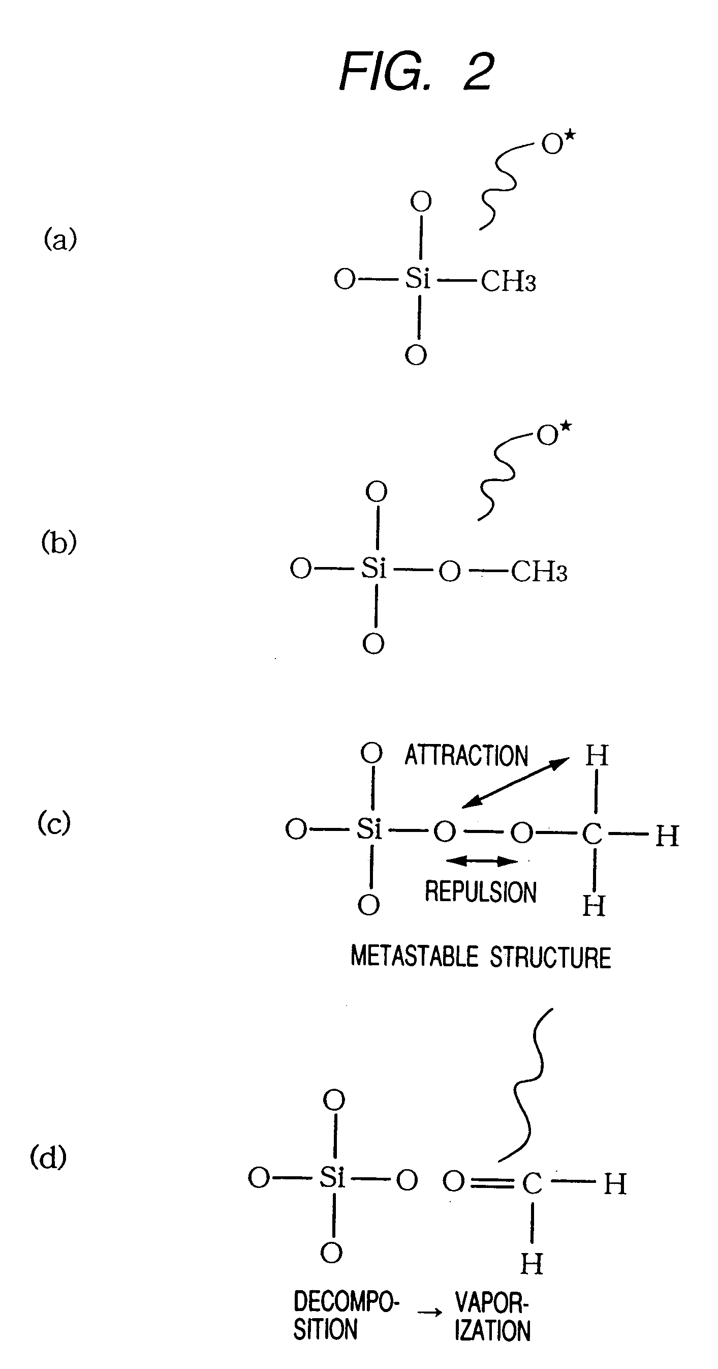
[0440] This Embodiment 1 specifically describes one of the technical concepts of the present invention, which comprises subjecting an insulating film, including an organosiloxane as a main component (the insulating film may hereinafter be called “organic insulating film”), to plasma etching in a gas atmosphere containing a fluorocarbon gas and a nitrogen gas, thereby forming, in the insulating film, a recess, such as an interconnect-forming trench or hole.

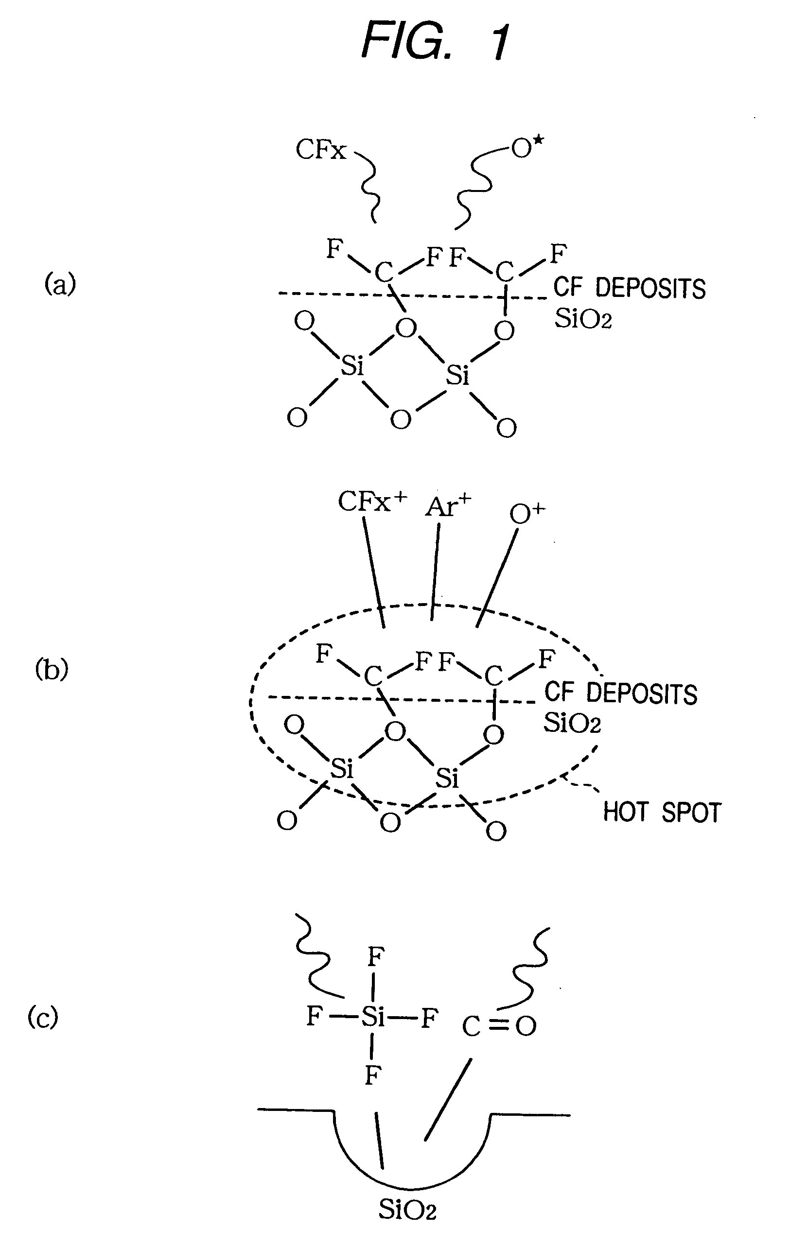
[0441] Prior to the description of this embodiment, various techniques and their problems which the present inventors have studied upon completion of this invention will be described first. FIGS. 1(a) to 1(c) schematically illustrate the etching principle, based on which a silicon oxide film (ex. SiO2) ordinarily employed as an interlevel dielectric film material of a semiconductor integrated circuit device is subjected to plasma dry etching in a gas atmosphere containing a fluorocarbon (CxFy) gas, oxygen (O2) gas and an argon (Ar...

embodiment 2

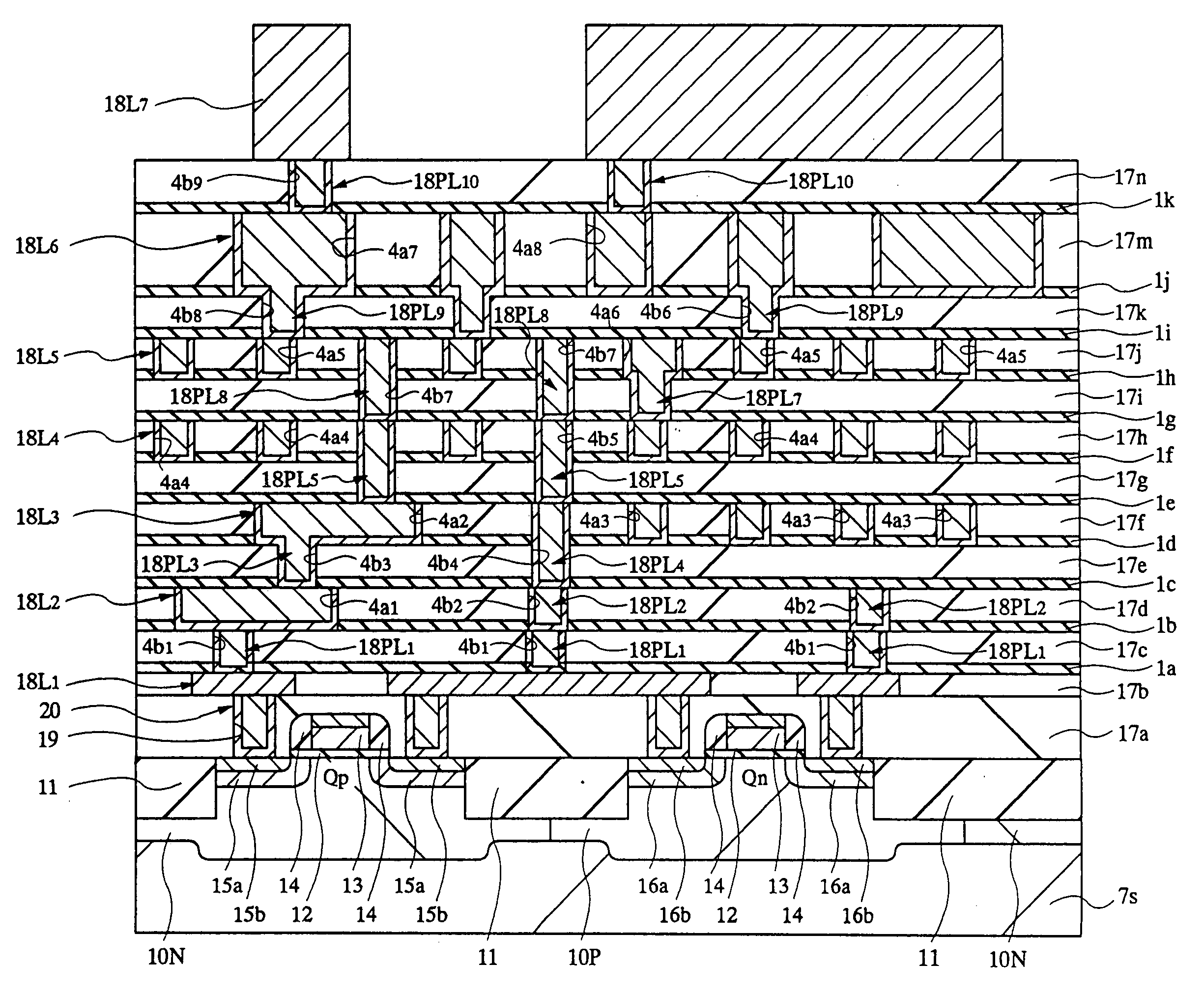
[0512] In this Embodiment 2, a modified example of the Embodiment 1 will be described, and, more specifically, application of the technical concept of the present invention to a dual damascene process different from that described in Embodiment 1 will be described. The manufacturing process of a semiconductor integrated circuit device according to Embodiment 2 will be described based on FIGS. 37(a) to 42(b), which show the semiconductor integrated circuit device of FIG. 14 during successive steps in the manufacture thereof.

[0513] Over the insulating film 1d as illustrated in FIG. 27(b), an interlevel dielectric film 17f is formed, as illustrated in FIG. 37(a) and FIG. 37(b). In this Embodiment 2, a silicon nitride film is used as a material of the insulating film 1d, as in Embodiment 1, but instead of it, a silicon oxide film formed, for example, by plasma CVD by using a TEOS gas to have a thickness of about 100 nm can be used. This interlevel dielectric film 17f has an organic ins...

embodiment 3

[0519] In this Embodiment 3, a modified example of Embodiment 1 or 2 will be described, and, more specifically, application of the technical concept of the present invention to a dual damascene process different from that described in Embodiment 1 or 2 will be described. The manufacturing process of the semiconductor integrated circuit device according to Embodiment 3 will be described based on FIGS. 43(a) to 50(b), which show the semiconductor integrated circuit device of FIG. 14 during successive steps in the manufacture thereof.

[0520] Over the insulating film 17f illustrated in FIG. 37(b), an insulating film 22 made of, for example, a silicon nitride film is formed, as illustrated in FIG. 43(a) and FIG. 43(b). This insulating film 22 is an etching mask member for formation of a trench or hole, and its thickness is about 150 nm. The insulating film 22 is not limited to a silicon nitride film, but can be changed variously. A film made of titanium nitride, tantalum, tantalum nitrid...


PUM


Abstract

In a process for the manufacture of a semiconductor integrated circuit device having an inlaid interconnect structure by embedding a conductor film in a recess, such as a trench or hole, formed in an organic insulating film which constitutes an interlevel dielectric film and includes an organosiloxane as a main component, the recess, such as a trench or hole, is formed by subjecting the organic insulating film to plasma dry etching in a CF-based gas/N2/Ar gas in order to suppress the formation of an abnormal shape on the bottom of the recess, upon formation of a photoresist film over the organic insulating film, followed by formation of the recess therein with the photoresist film as an etching mask.

Description

CROSS REFERENCE TO RELATED APPLICATION [0001] This application is a continuation of U.S. application Ser. No. 09 / 646,671, filed Sep. 20, 2000, the contents of which are incorporated herein by reference in their entirety. Application Ser. No. 09 / 646,671 is a National Stage application filed under 35 USC 371 of International (PCT) Application No. PCT / JP00 / 04046, filed Jun. 21, 2000.TECHNICAL FIELD [0002] This invention relates to a process and technique for the manufacture of a semiconductor integrated circuit device, particularly, to a technique which is effective when adapted to a multilevel metallization process in the manufacture of a semiconductor integrated circuit device. BACKGROUND OF THE INVENTION [0003] In line with improvements in the degree of element integration or in the reduction in the size of a semiconductor chip in a semiconductor integrated circuit device, miniaturization and multilevel fabrication of interconnects constituting the semiconductor integrated circuit d...

Claims


Application Information

Patent Timeline
Patent Type & Authority Applications(United States)
IPC IPC(8): H01L21/3065H01L21/311H01L21/312H01L21/44H01L21/4763H01L21/768H01L23/52H01L29/40
CPCH01L21/3065H01L21/31116H01L21/31138H01L21/31144H01L21/3122H01L21/76802H01L21/76835H01L21/76808H01L21/7681H01L21/76811H01L21/76813H01L21/76829H01L21/76807H01L21/022H01L21/02126H01L21/0217H01L21/768
Inventor UNO, SHOUOCHIMAEKAWA, ATSUSHIYUNOGAMI, TAKASHITAGO, KAZUTAMINOJIRI, KAZUOMACHIDA, SHUNTAROTOKUNAGA, TAKAFUMI
Owner RENESAS ELECTRONICS CORP
Why Eureka
Try Eureka