Semiconductor device having an etch stopper formed of a sin layer by low temperature ALD and method of fabricating the same

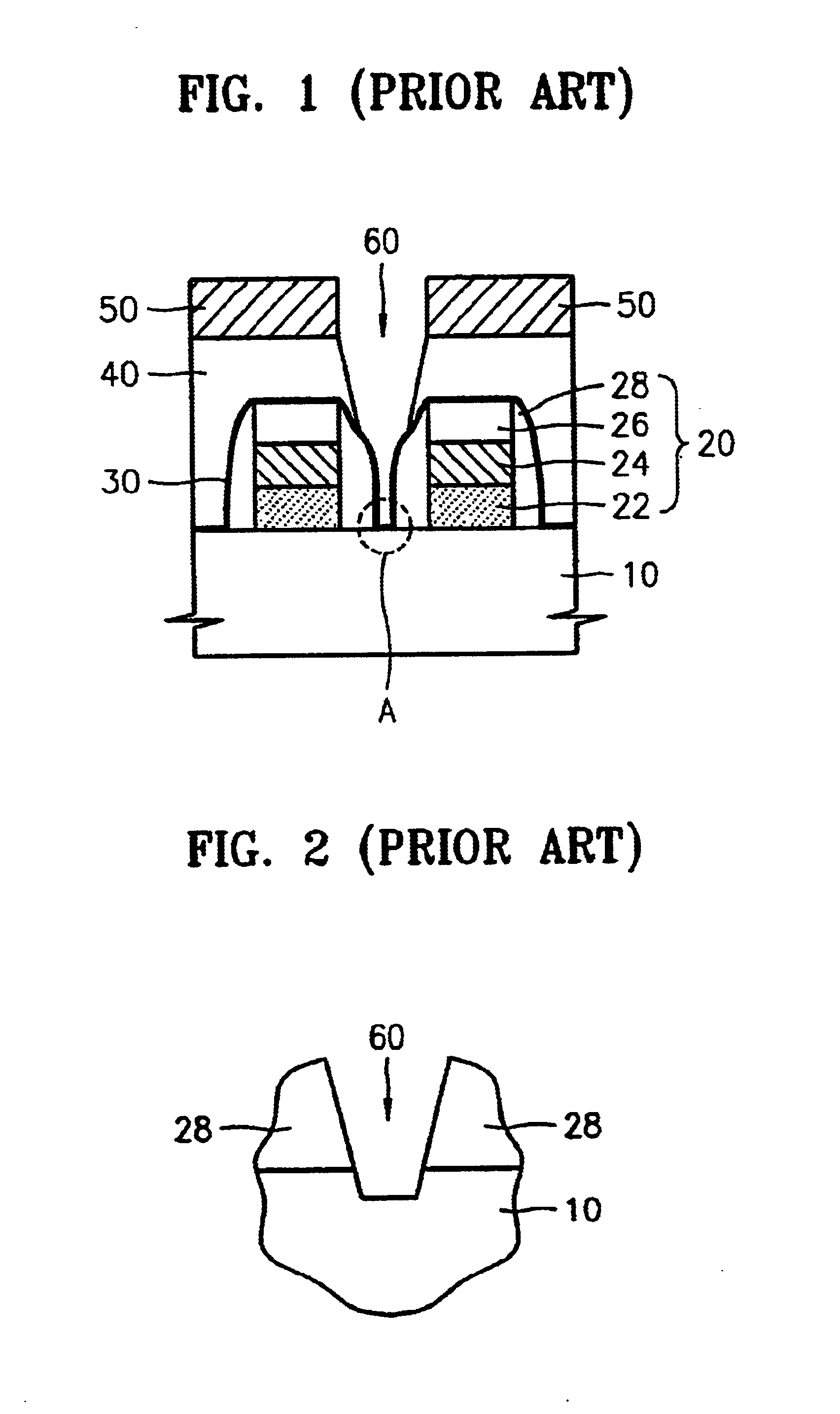
a technology of etch stopper and semiconductor, which is applied in the direction of semiconductor devices, electrical devices, transistors, etc., can solve the problems of inability to control the thickness of the nitride film to be constant, the thickness of the nitride film is very thin, and the etching speed is not yet constant, so as to prevent the formation of a recess and prevent damage to the semiconductor substrate

Inactive Publication Date: 2005-02-22
SAMSUNG ELECTRONICS CO LTD
View PDF4 Cites 66 Cited by
  • Summary
  • Abstract
  • Description
  • Claims
  • Application Information

AI Technical Summary

Benefits of technology

The present invention provides a semiconductor device having an etch stopper formed of a nitride film by low temperature atomic layer deposition (ALD) so as to prevent damage to a semiconductor substrate and prevent a recess from forming therein.

Problems solved by technology

This is because the film to be etched is very thin, and a constant etching speed for the whole wafer is not yet possible.
Further, the thickness of the nitride film cannot be controlled to be constant.
In addition, since there are differences among equipment used for mass production, it is difficult to consistantly etch thin films, a fact which causes further damage to semiconductor substrates.
Damage to the semiconductor substrate 10 or a recess therein can cause AC parameter defects such as TRDL (last data in to row precharge) in the DRAM device chip at the center of the wafer which has been etched less while degrading the refresh characteristics at the edge of the wafer which has been etched more.

Method used


Image

  • Semiconductor device having an etch stopper formed of a sin layer by low temperature ALD and method of fabricating the same
  • Semiconductor device having an etch stopper formed of a sin layer by low temperature ALD and method of fabricating the same
  • Semiconductor device having an etch stopper formed of a sin layer by low temperature ALD and method of fabricating the same

Examples


Embodiment Construction

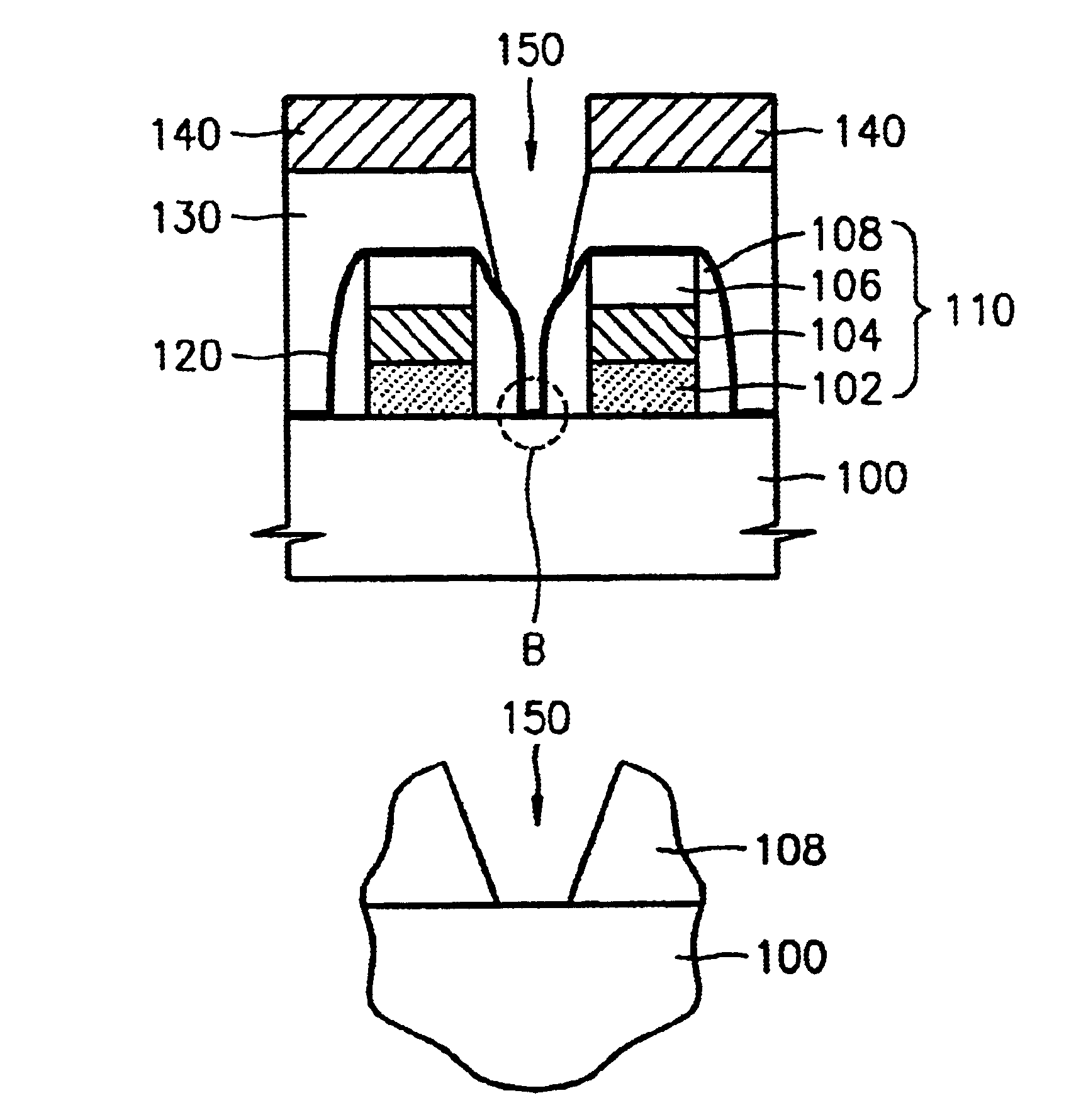
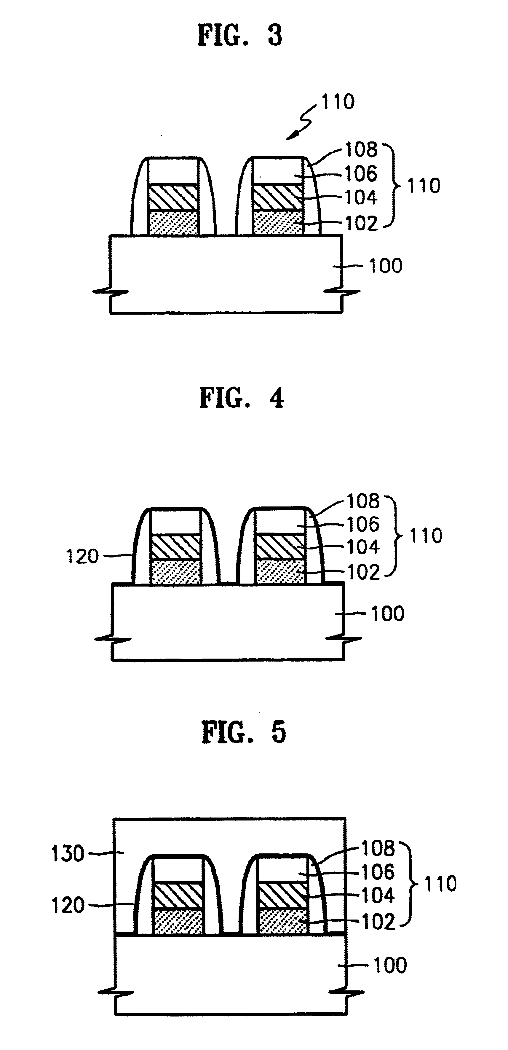
The present invention now will be described more fully with reference to the accompanying drawings, in which preferred embodiments of the invention are shown. This invention may, however, be embodied in many different forms and should not be construed as being limited to the embodiments set forth herein. Various embodiments may be implemented without departing from the spirit and the essential characteristics of the invention as defined by the appended claims. For example, in a preferred embodiment of the present invention, an etch stopper formed of a second nitride film by low temperature atomic layer deposition (ALD) (i.e., under 500° C.) is applied or used on a gate pattern in a SAC process. The second nitride film can also be used as an etch stopper in other processes. Therefore, the following examples are for illustrative purposes and are not intended to limit the scope of the invention.

Referring to FIG. 5, a semiconductor device having an etch stopper formed of a nitride film ...


PUM

PropertyMeasurementUnit
temperatureaaaaaaaaaa

Abstract

Provided are a semiconductor device having an etch stopper formed of a nitride film by low temperature atomic layer deposition which can prevent damage to a semiconductor substrate and a method for fabricating the semiconductor device. Damage to the semiconductor substrate under the etch stopper composed of a second nitride film can be prevented by forming a first nitride film using high temperature LPCVD on the semiconductor substrate, forming the etch stopper including the second nitride film by low temperature ALD on the first nitride film, and removing the second nitride film by dry etching, thus taking advantage of the different etch selectivities of the first nitride film and the second nitride film.

Description

BACKGROUND OF THE INVENTIONThis application claims the priority of Korean Patent Application No. 2002-55005, filed on Sep. 11, 2002, in the Korean Intellectual Property Office, the contents of which are incorporated herein in their entirety by reference.1. Field of the InventionThe present invention relates to a semiconductor device and a method for fabricating the semiconductor device, and more particularly, to a semiconductor device having an etch stopper formed of a silicon nitride (SiN) layer by low-temperature atomic layer deposition (ALD) in a self-aligned contact (SAC) process and a method for fabricating the semiconductor device.2. Description of the Related ArtAs a finer pattern and a thinner film are required in a process of fabricating semiconductor devices, atomic layer deposition (ALD) technology beneficial for the finer pattern and the thinner film is more widely applied to DRAM devices. In particular, ALD is useful for accurately controlling the thickness of a film an...

Claims


Application Information

Patent Timeline
Patent Type & Authority Patents(United States)
IPC IPC(8): H01L21/02H01L21/311H01L21/28H01L21/3065H01L21/318H01L21/60H01L21/768H01L21/8234H01L21/8242H01L27/088H01L27/108
CPCH01L21/31111H01L21/76897H01L21/31116H01L21/28
Inventor CHU, KANG-SOOLEE, J O-WONPARK, JAE-EUNYANG, JONG-HO
Owner SAMSUNG ELECTRONICS CO LTD
Why Eureka
Try Eureka