
Thermal processing apparatus
a technology of thermal processing apparatus and thermal processing apparatus, which is applied in the direction of lighting and heating apparatus, applications, furniture, etc., can solve the problems of insufficient annealing process of a higher temperature, the provision of such bulky shutting mechanism, and the structure of the thermal processing apparatus, so as to improve the heating efficiency of the object, the effect of rapid increase and decrease of the temperature of the obj
- Summary
- Abstract
- Description
- Claims
- Application Information
AI Technical Summary
Benefits of technology
Problems solved by technology
Method used
Image

Examples
first embodiment
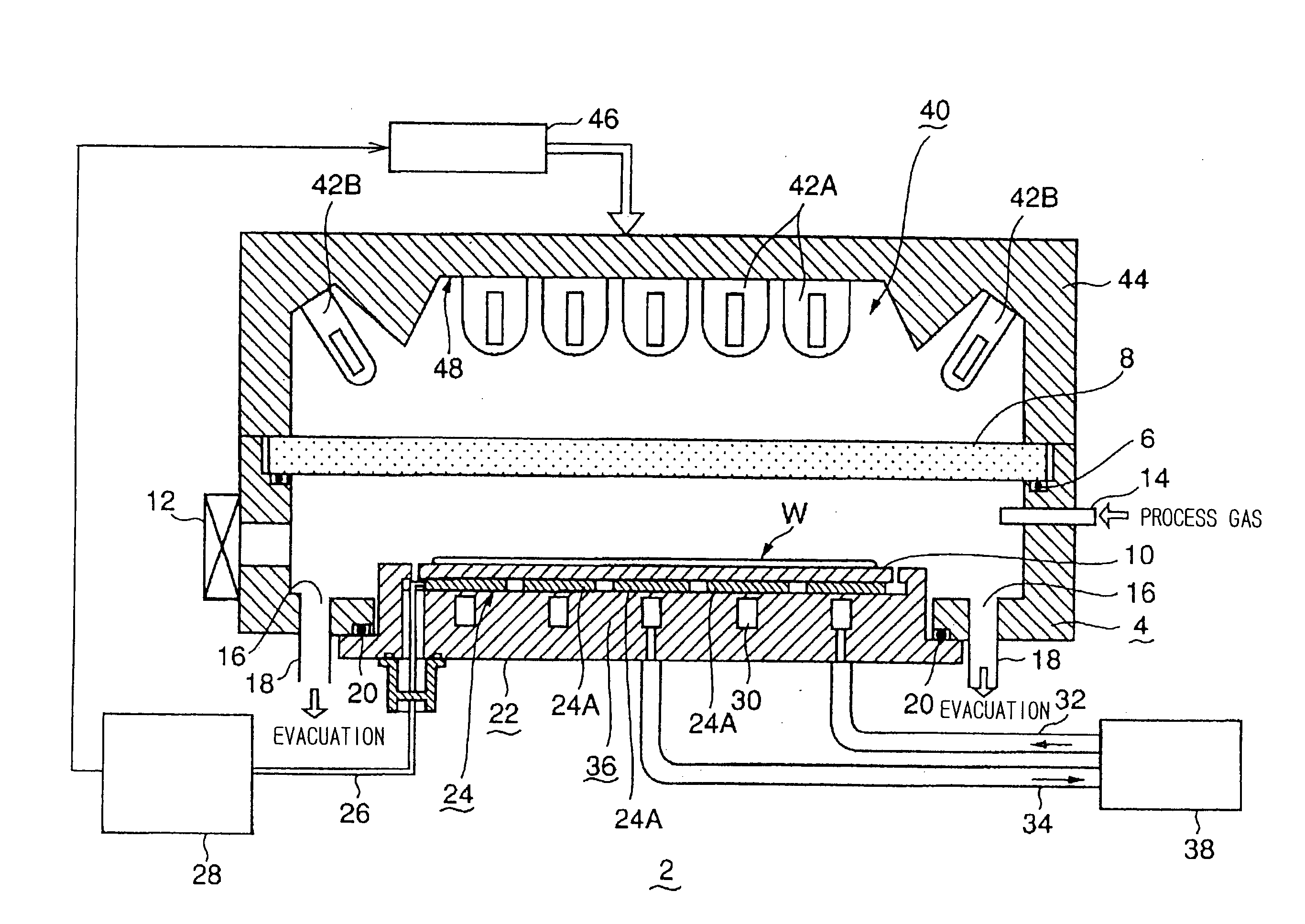
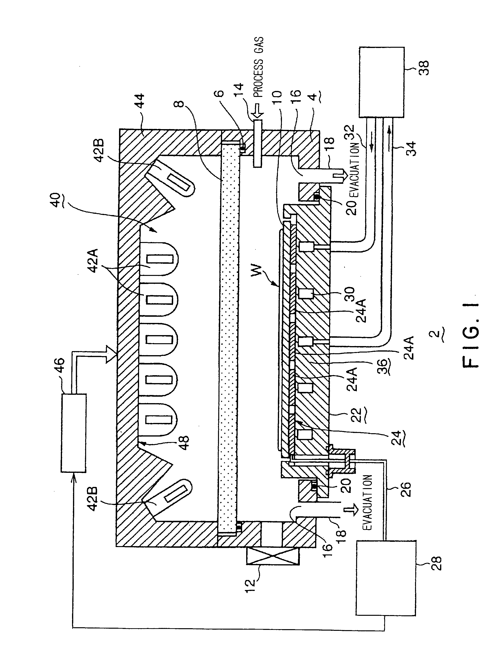
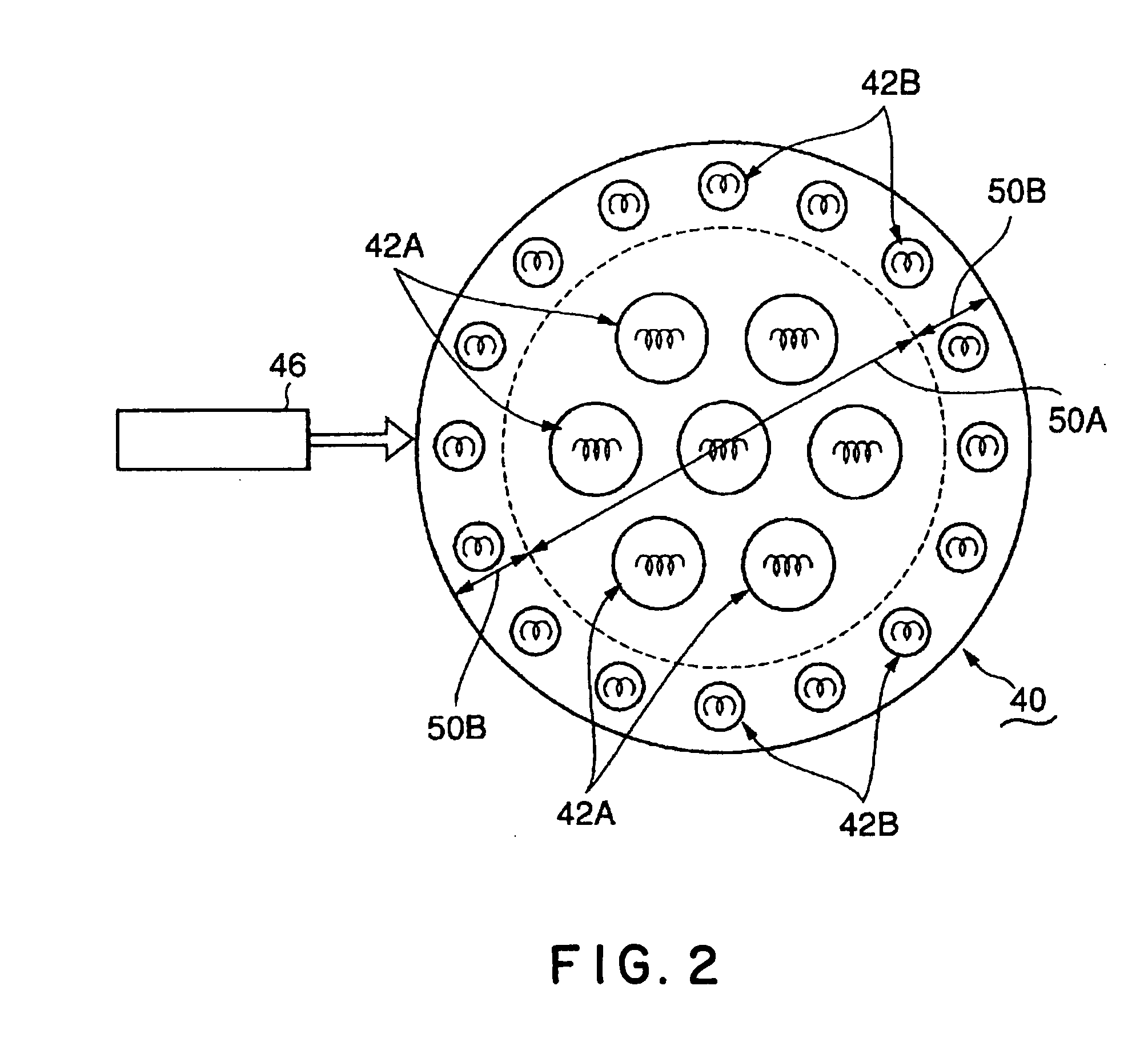
[0045]As shown in FIG. 1, a thermal processing apparatus 2 in a first embodiment of the present invention includes a cylindrical processing vessel 4 made of, e.g., aluminum. A top part of the processing vessel 4 is opened, and a transparent transmitting window 8 is air-tightly fitted in the top opening through a sealing member 6 such as an O-ring. A thin disk-shaped table 10 is disposed in the processing vessel 4. An object to be processed such as a semiconductor wafer W is supported on an upper surface of the table 10. The table 10 is formed of such a material that is best suited for absorbing a light ray irradiated from a heat lamp to be used. For example, the table 10 is formed of an SiO2 material, an AlN material, or an SiC material, which tends to mainly absorb a light ray from an infrared lamp. Alternatively, the table 10 is formed of a Ge (germanium) material, an Si material, or a metal material, which tends to mainly absorb a light ray from an ultraviolet lamp or a halogen l...
second embodiment
[0073]In the first embodiment, the table 10 is formed of a single material, but the present invention is not limited thereto. For example, the table 10 may be formed by stacking a plurality of absorbing plates having different main absorption wavelength bands.
[0074]FIG. 10 shows schematic views (A) and (B) of structures of a table in a second embodiment of the present invention. Illustration of structures other than the table 10 are omitted. Specifically, the table 10 is manufactured by stacking a visible-ray absorbing plate 62 that mainly absorbs the ultraviolet ray and the visible ray, and an infrared-ray absorbing plate 64 that mainly absorbs the infrared ray.
[0075]Regarding materials constituting the respective absorbing plates 62 and 64, the ultraviolet and visible-ray absorbing plate 62 may be a germanium plate or a silicon plate, for example, while the infrared-light absorbing plate 64 may be a quartz plate, an AlN plate, or an SiC plate, which has been as stated above referr...
third embodiment
[0079]Next, a third embodiment of the present invention is described below. FIG. 11 is a schematic sectional view of the third embodiment of the present invention. The same parts as those of FIG. 1 are depicted by the same reference numbers, and their description is omitted. As shown in FIG. 11, a reflecting plate 70 made of aluminum plating is disposed to cover all the upper surface of a heat-medium jacket 36 serving as a base plate 22 of a processing vessel 4. A table 10 is disposed on the reflecting plate 70 through Peltier elements 24A.
[0080]In the third embodiment, a heat ray that has transmitted a wafer W and the table 10 is reflected upward by the reflecting plate 70, and thus the heat ray again contributes to heating of the wafer W. Since the heating efficiency can be improved because of the reflected ray, the wafer can be more rapidly heated. It goes without saying that the structures of the second embodiment shown in FIG. 10(A) and FIG. 10(B) can be applied to the table 10...
PUM
| Property | Measurement | Unit |
|---|---|---|
| temperature | aaaaa | aaaaa |
| temperature | aaaaa | aaaaa |
| temperature | aaaaa | aaaaa |
Abstract
Description
Claims
Application Information