Capacitance device and resonance circuit

a capacitor and resonance circuit technology, applied in the direction of fixed capacitor details, variable capacitors, stacked capacitors, etc., can solve the problem that the control voltage necessary for changing the capacitance of the variable capacitor cannot be stably manufactured, the intensity of the electric field applied to the dielectric layer decreases, and the change of the capacitance due to the displacement of the electrodes across the dielectric layer. , to achieve the effect of suppressing the change of capacitance, stable manufacturing of the capaci

Active Publication Date: 2011-07-07
DEXERIALS CORP
View PDF5 Cites 24 Cited by
  • Summary
  • Abstract
  • Description
  • Claims
  • Application Information

AI Technical Summary

Benefits of technology

[0016]The present invention has been made to solve the above problem, and it is an object of the present invention to suppress changes in capacitance due to displacement between electrodes opposing each other across a dielectric layer, thereby allowing stable manufacturing of a capacitance device having a desired capacitance.
[0017]To solve the above problem, a capacitance device according to the present invention includes a dielectric layer, a first electrode formed on a predetermined surface of the dielectric layer, and a second electrode formed on an opposite surface of the dielectric layer opposite to the predetermined surface. The first electrode is formed in a predetermined first shape. The second electrode has a first region overlapping a projection pattern obtained by projecting the first electrode onto the opposite surface, and is formed in a second shape such that the area of the first region does not change even when the first electrode undergoes relative displacement in a predetermined direction within the predetermined surface.
[0018]With the present invention, even when the first electrode undergoes relative displacement in a predetermined direction with respect to the second electrode, the area of the region (first region) in which the projection pattern obtained by projecting the first electrode onto the second electrode side, and the second electrode overlap each other does not change. Therefore, according to an embodiment of the present invention, changes in capacitance due to displacement between electrodes formed across a dielectric layer can be suppressed, thereby allowing stable manufacturing of a capacitance device having a desired capacitance.

Problems solved by technology

However, an increase in the thickness of the dielectric layer causes a decrease in the intensity of the electric field applied to the dielectric layer, so the control voltage necessary for changing the capacitance of the variable capacitance device becomes high.
As a result, there is a problem that capacitance variations among individual variable capacitance devices become large, so a variable capacitance device having a desired capacitance cannot be stably manufactured.
Further, the problem of capacitance variations among individual variable capacitance devices is not restricted to variable capacitance devices, and occurs similarly with capacitance devices regarding which the capacitance hardly changes at all, regardless of the type of input signal (AC or DC) and the signal level thereof.

Method used


Image

  • Capacitance device and resonance circuit
  • Capacitance device and resonance circuit
  • Capacitance device and resonance circuit

Examples


first embodiment

1. First Embodiment

[0081]In a first embodiment, a description will be given of an example of two-terminal type variable capacitance device with no control terminal additionally provided to control changes in capacitance.

[Influence of Displacement Between Electrodes]

[0082]Before describing the configuration of a variable capacitance device according to this embodiment, first, the above-described problem of displacement which is to be solved by the present invention will be described more specifically with reference to the drawings.

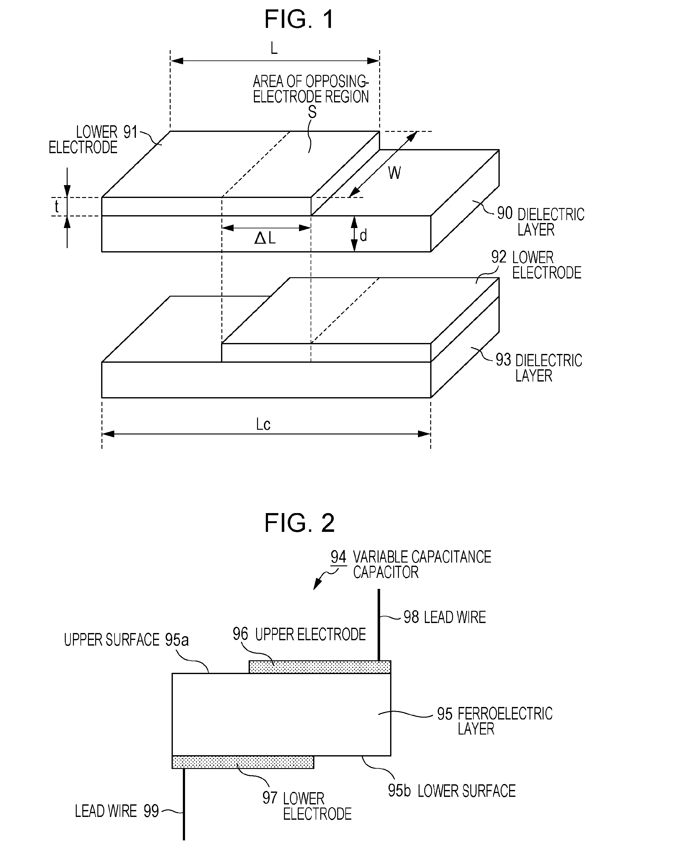
[0083]FIG. 1 shows the schematic configuration of a typical layered variable capacitance capacitor. An exploded view of the layered variable capacitance capacitor is shown in FIG. 1. The layered variable capacitance capacitor has a configuration in which a layer formed by a dielectric layer 90 and an upper electrode 91 formed on the dielectric layer 90, and a layer formed by a dielectric layer 93 and an lower electrode 92 formed on the dielectric layer 93 a...

modification 1

[Modification 1]

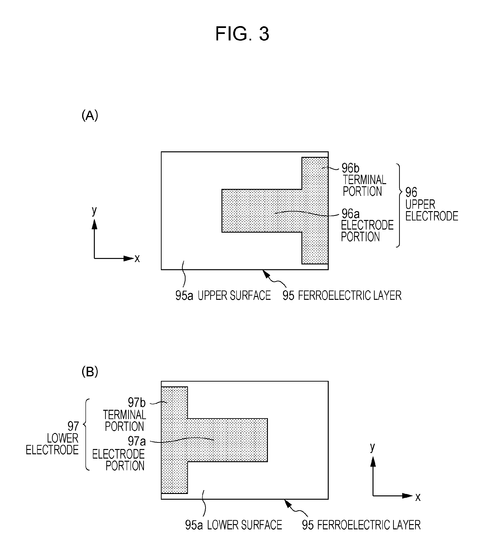
[0138]While description has been made in the above first embodiment relating to the case in which the extending direction (x direction) of the electrode portion 11a of the upper electrode 11 and the extending direction (y direction) of the electrode portion 12a of the lower electrode 12 are orthogonal to each other, the present invention is not limited to this. In Modification 1, a description will be given of an example of configuration in which the extending direction of the electrode portion of the upper electrode and the extending direction of the electrode portion of the lower electrode are not orthogonal to each other.

[Electrode Configuration]

[0139]FIGS. 13(A) and (B) show the configurations of an upper electrode and lower electrode of a variable capacitance capacitor according to Modification 1, respectively. FIGS. 13(A) and (B) are a top view and a bottom view of the variable capacitance capacitor according to Modification 1, respectively. Modification 1 is o...

modification 2

[Modification 2]

[0158]Modification 1 mentioned above relates to the case in which the terminal portions of the upper electrode and lower electrode are formed along the extending direction (y direction) of the short sides of the upper and lower surfaces of the ferroelectric layer, and near the short sides. However, the present invention is not limited to this. In Modification 2, a description will be given of a case in which the terminal portions of the upper electrode and lower electrode are formed along the extending direction (x direction) of the long sides of the upper and lower surfaces of the ferroelectric layer, and near the long sides.

[Electrode Configuration]

[0159]FIGS. 17(A) and (B) show the configurations of an upper electrode and lower electrode according to Modification 2, respectively. FIGS. 17(A) and (B) are a top view and a bottom view of a variable capacitance capacitor according to Modification 2, respectively. Modification 2 is of the same configuration as the vari...


PUM


Abstract

To suppress changes in capacitance due to displacement between electrodes opposing each other across a dielectric layer, thereby allowing stable manufacturing of a capacitance device having a desired capacitance.
The capacitance device according to the present invention is of a configuration including a dielectric layer (10), a first electrode (11) formed on a predetermined surface (10a) of the dielectric layer (10), and a second electrode (12) formed on a surface (10b) on the opposite side of the dielectric layer (10) from the predetermined surface (10a). The forms of the first and second electrodes (11, 12) are set so that even in the event that the first electrode (11) is relatively displaced regarding position in a predetermined direction as to the second electrode (12), the area of the opposing-electrode region between the first electrode (11) and to the second electrode (12) is unchanged.

Description

TECHNICAL FIELD[0001]The present invention relates to a capacitance device and a resonance circuit including the same, and more specifically to a capacitance device and a resonance circuit including the same, having a small capacitance in pF order, for example.BACKGROUND ART[0002]Conventionally, variable capacitance devices have been used whose capacitance is changed by application of external bias signals to thereby control the frequency, time period, or the like of an input signal. Such variable capacitance devices have been made commercially available as, for example, variable capacitance diodes (varicaps) and MEMS (Micro Electro Mechanical Systems).[0003]In addition, conventionally, there has been proposed a technique for using the above-described variable capacitance device as a protection circuit in a non-contact IC (Integrated Circuit) card (see, for example, PTL 1). According to the technique described in PTL 1, a variable capacitance device is used as a protection circuit i...

Claims


Application Information

Patent Timeline
Patent Type & Authority Applications(United States)
IPC IPC(8): H03H7/00H01G5/16H01G7/06
CPCH01G4/255H01G4/30H03H7/0115H01G7/00H01G7/06H03H2001/0085H01G4/232
Inventor KANNO, MASAYOSHIYOKOTA, TOSHIAKIHABU, KAZUTAKAWATANABE, MAKOTOSATO, NORITAKA
Owner DEXERIALS CORP
Why Eureka
Try Eureka