Field Effect Transistor Device with Self-Aligned Junction and Spacer
a field effect transistor and self-aligning junction technology, which is applied in the direction of semiconductor devices, basic electric elements, electrical equipment, etc., can solve the problems of increasing the parasitic capacitance of the fets and the device affecting the parasitic capacitance in the devi
- Summary
- Abstract
- Description
- Claims
- Application Information
AI Technical Summary
Problems solved by technology
Method used
Image


Examples
Embodiment Construction
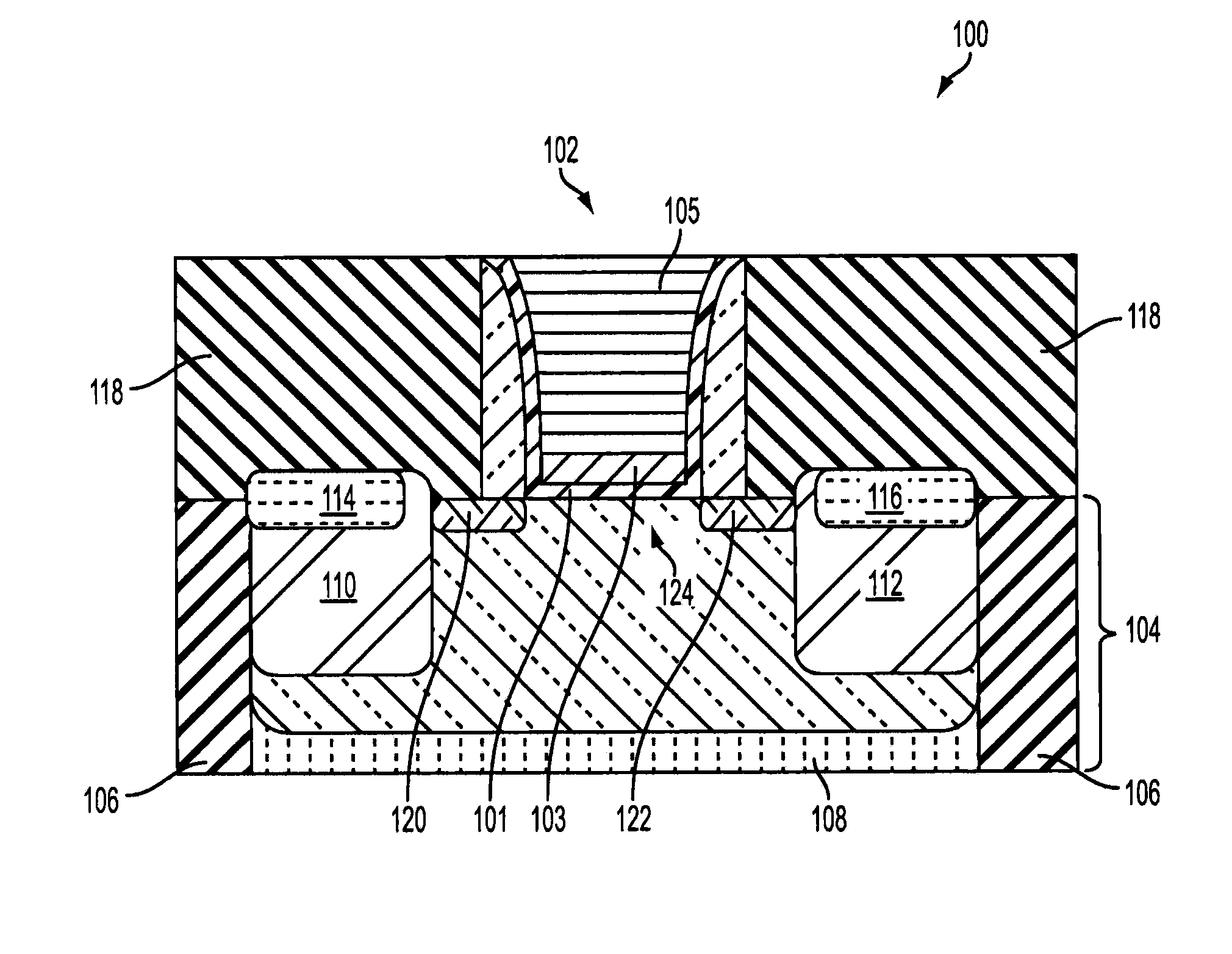
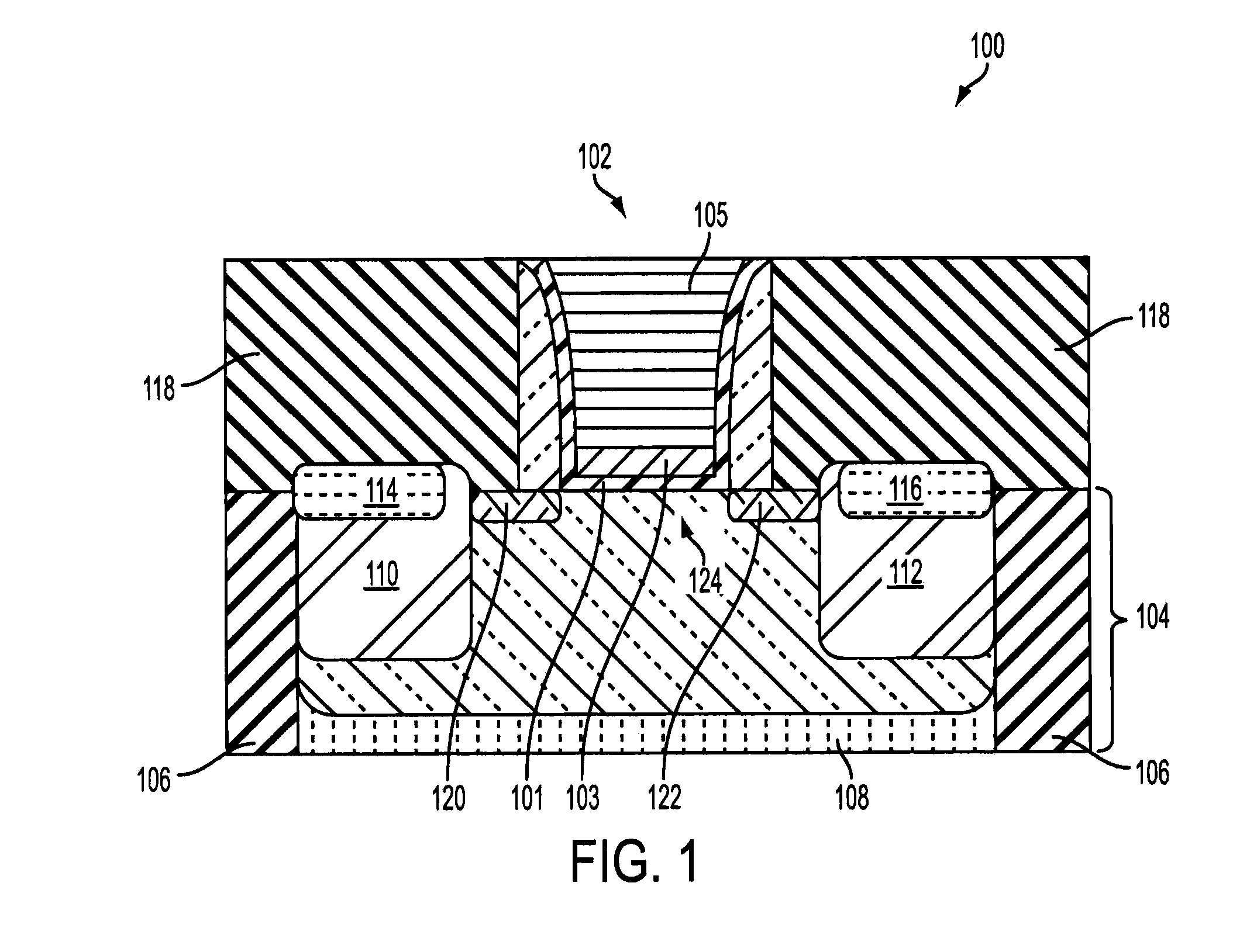
[0016]FIG. 1 illustrates a side cut-away view of an exemplary embodiment of a field effect transistor (FET) device 100. The device 100 includes a gate stack portion 102 disposed on channel region 124 of a substrate 104. The gate stack portion 102 may include, for example layer 101 disposed on the substrate 104, and a layer 103 disposed on the layer 101. The layer 101 may include a dielectric material, such as silicon dioxide or a high-k layer of material. The layer 103 may include a polysilicon material or a metallic gate material. A capping layer 105 including, for example, a polysilicon material may be disposed on the layer 103. The substrate 104 may include for example a silicon trench isolation (STI) portion 106 and a buried oxide portion 108.
[0017]The device 100 includes a source region 110 and a drain region 112. The source and drain regions 110 and 112 may be formed from epitaxially grown silicon material including, for example, SiC for nFET, SiGe for pFET. The source and dra...
PUM
 Abstract
Description
Claims
Application Information