Supercharge Your Innovation With Domain-Expert AI Agents!

Photovoltaic device including flexible or inflexible substrate and method for manufacturing the same

a photovoltaic device and flexible or inflexible technology, applied in the field of photovoltaic devices, can solve the problems of significant light exposure damage to the substrate, and the fatal disadvantage of hydrogenated amorphous silicon (a-si:h)

Inactive Publication Date: 2012-12-27
INTELLECTUAL DISCOVERY CO LTD
View PDF3 Cites 0 Cited by
  • Summary
  • Abstract
  • Description
  • Claims
  • Application Information

AI Technical Summary

Benefits of technology

The proposed structure and manufacturing method result in a photovoltaic device with improved quantum efficiency and reduced recombination loss, enhancing the photoelectric conversion efficiency and stability of the device.

Problems solved by technology

That is to say, the hydrogenated amorphous silicon (a-Si:H) has a fatal disadvantage of significant degradation by light exposure.

Method used


Image

  • Photovoltaic device including flexible or inflexible substrate and method for manufacturing the same
  • Photovoltaic device including flexible or inflexible substrate and method for manufacturing the same
  • Photovoltaic device including flexible or inflexible substrate and method for manufacturing the same

Examples


Embodiment Construction

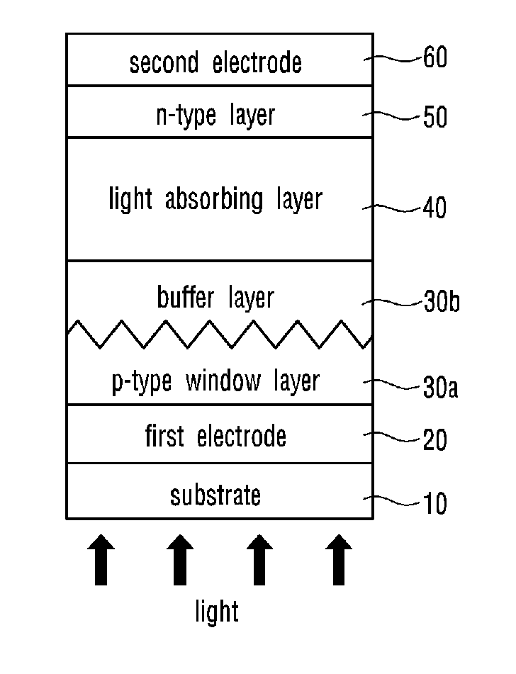
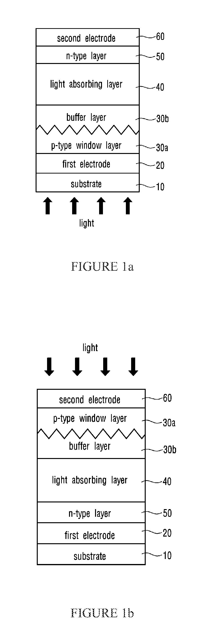
[0012]Hereinafter, said silicon thin film photovoltaic device and a method for manufacturing the same will be described in detail with reference to the accompanying drawings.

[0013]FIGS. 1a and 1b are cross sectional views of a p-i-n type thin film photovoltaic device and an n-i-p type thin film photovoltaic device according to an embodiment of the present invention.

[0014]As shown in FIGS. 1a and 1b, a photovoltaic device according to the embodiment of the present invention includes a substrate 10, a first electrode 20, a p-type window layer 30a, a buffer layer 30b, a light absorbing layer 40, an n-type layer 50 and a second electrode 60.

[0015]The photovoltaic device according to the embodiment of the present invention includes the p-type window layer 30a, buffer layer 30b, light absorbing layer 40 and n-type layer 50, which are sequentially stacked from an electrode on which light is first incident among the first electrode 20 and the second electrode 60.

[0016]That is, in the p-i-n ...


PUM

PropertyMeasurementUnit
thicknessaaaaaaaaaa
thicknessaaaaaaaaaa
thicknessaaaaaaaaaa

Abstract

Disclosed is a photovoltaic device. The photovoltaic device according to the present invention includes: a first electrode; a second electrode; and a p-type window layer, a buffer layer, a light absorbing layer and an n-type layer, which are sequentially stacked between the first electrode and the second electrode, wherein, when the p-type window layer is composed of hydrogenated amorphous silicon oxide, the buffer layer is composed of either hydrogenated amorphous silicon carbide or hydrogenated amorphous silicon oxide, and wherein, when the p-type window layer is composed of hydrogenated amorphous silicon carbide, the buffer layer is composed of hydrogenated amorphous silicon oxide.

Description

CROSS-REFERENCE TO RELATED APPLICATIONS[0001]This application is a divisional of U.S. patent application Ser. No. 13 / 071,191, filed on Mar. 24, 2011, which claims priority under 35 U.S.C. §119 to Korean Patent Application No. 10-2010-0027397, filed on Mar. 26, 2010, the entireties of which are hereby incorporated by reference.FIELD OF THE INVENTION[0002]The present invention relates to a photovoltaic device including a flexible substrate or an inflexible substrate and a method for manufacturing the same.BACKGROUND OF THE INVENTION[0003]Since an amorphous silicon (a-Si) photovoltaic device was first developed in 1976, it has been widely researched because hydrogenated amorphous silicon (a-Si:H) has a high photosensitivity in a visible light region, easy controllability of an optical band gap and processibility at a low price and a low temperature and of a wide area.[0004]However, it was discovered that the hydrogenated amorphous silicon (a-Si:H) suffers from Stabler-Wronski effect. T...

Claims


Application Information

Patent Timeline
Patent Type & Authority Applications(United States)
IPC IPC(8): H01L31/065H01L31/18
CPCH01L31/03765H01L31/03767Y02E10/548H01L31/202H01L31/204H01L31/075Y02P70/50
Inventor MYONG, SEUNG-YEOP
Owner INTELLECTUAL DISCOVERY CO LTD
Features
  • R&D
  • Intellectual Property
  • Life Sciences
  • Materials
  • Tech Scout
  • Unparalleled Data Quality
  • Higher Quality Content
  • 60% Fewer Hallucinations
Learn More