
LED package and method for making the same

a technology of light-emitting diodes and led packages, which is applied in the direction of semiconductor/solid-state device manufacturing, electrical apparatus, semiconductor devices, etc., can solve the problems of complex and difficult process of forming a reflective layer on the inner surface of the cup to define the receiving cavity, and the luminous efficiency of the led package is still not satisfactorily high

Inactive Publication Date: 2012-12-27
ADVANCED OPTOELECTRONICS TECH
View PDF6 Cites 35 Cited by
  • Summary
  • Abstract
  • Description
  • Claims
  • Application Information

AI Technical Summary

Benefits of technology

[0005]However, due to that the reflective layer being merely formed in the receiving cavity, the substrate does reflect light as a supplementary means for light reflection. Thus, the luminous efficiency of the LED package is still not satisfactorily high. Furthermore, the process of forming a reflective layer on the inner surface of the cup defining the receiving cavity is complex and difficult.

Problems solved by technology

Thus, the luminous efficiency of the LED package is still not satisfactorily high.
Furthermore, the process of forming a reflective layer on the inner surface of the cup defining the receiving cavity is complex and difficult.

Method used


Image

  • LED package and method for making the same
  • LED package and method for making the same
  • LED package and method for making the same

Examples


Embodiment Construction

[0013]Reference will now be made to the drawings to describe the present LED package, and method for making the LED package, in detail.

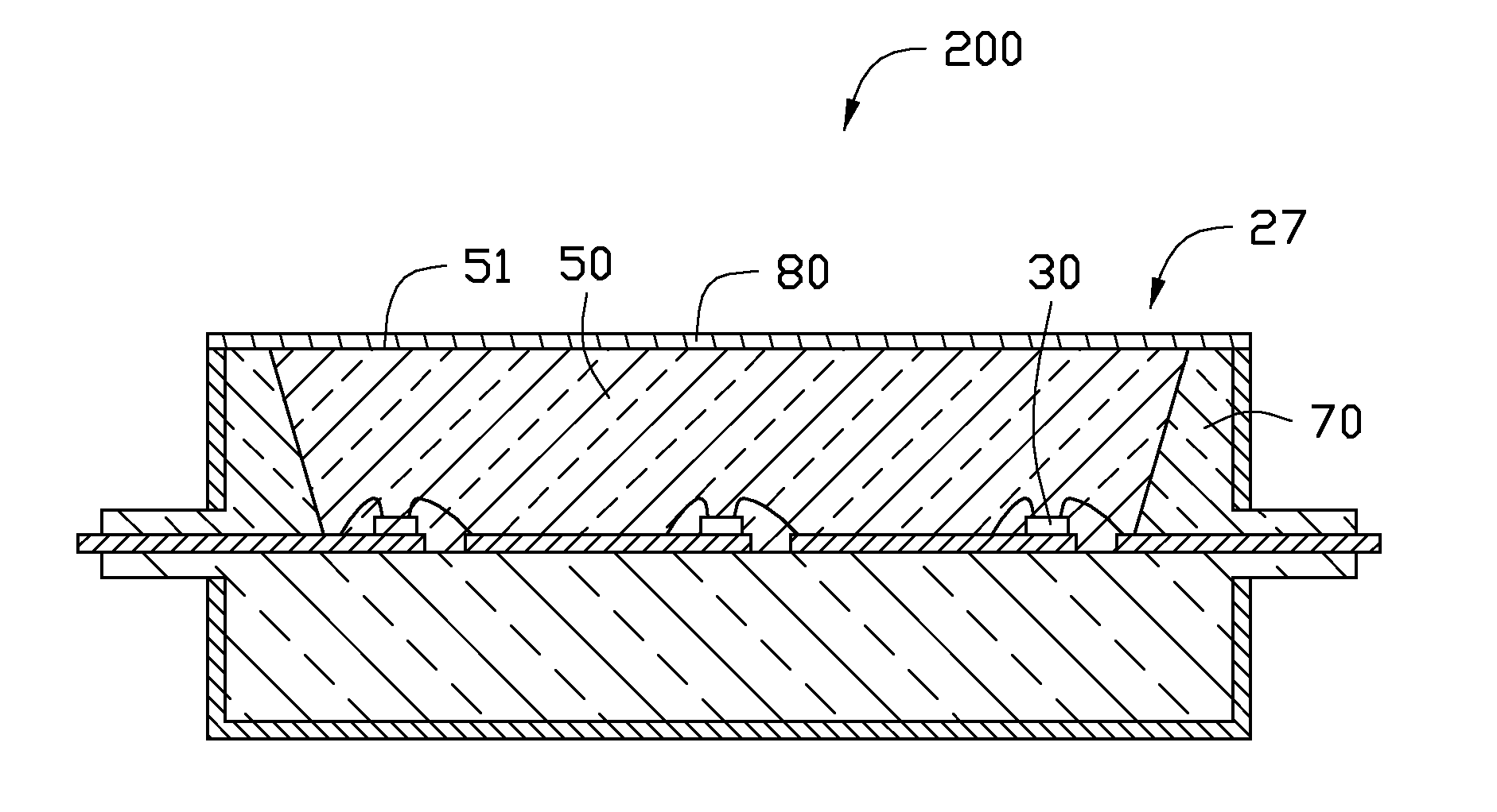
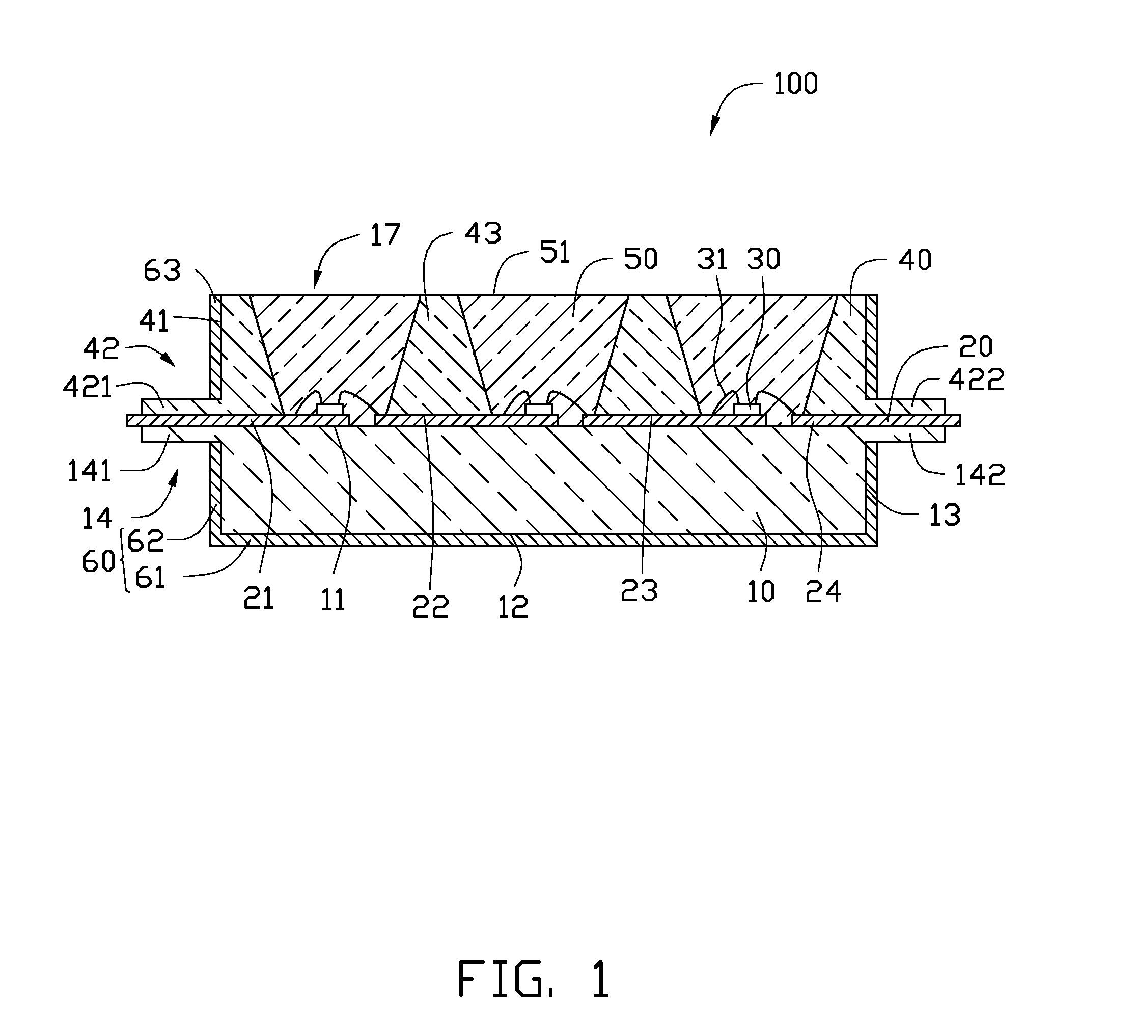
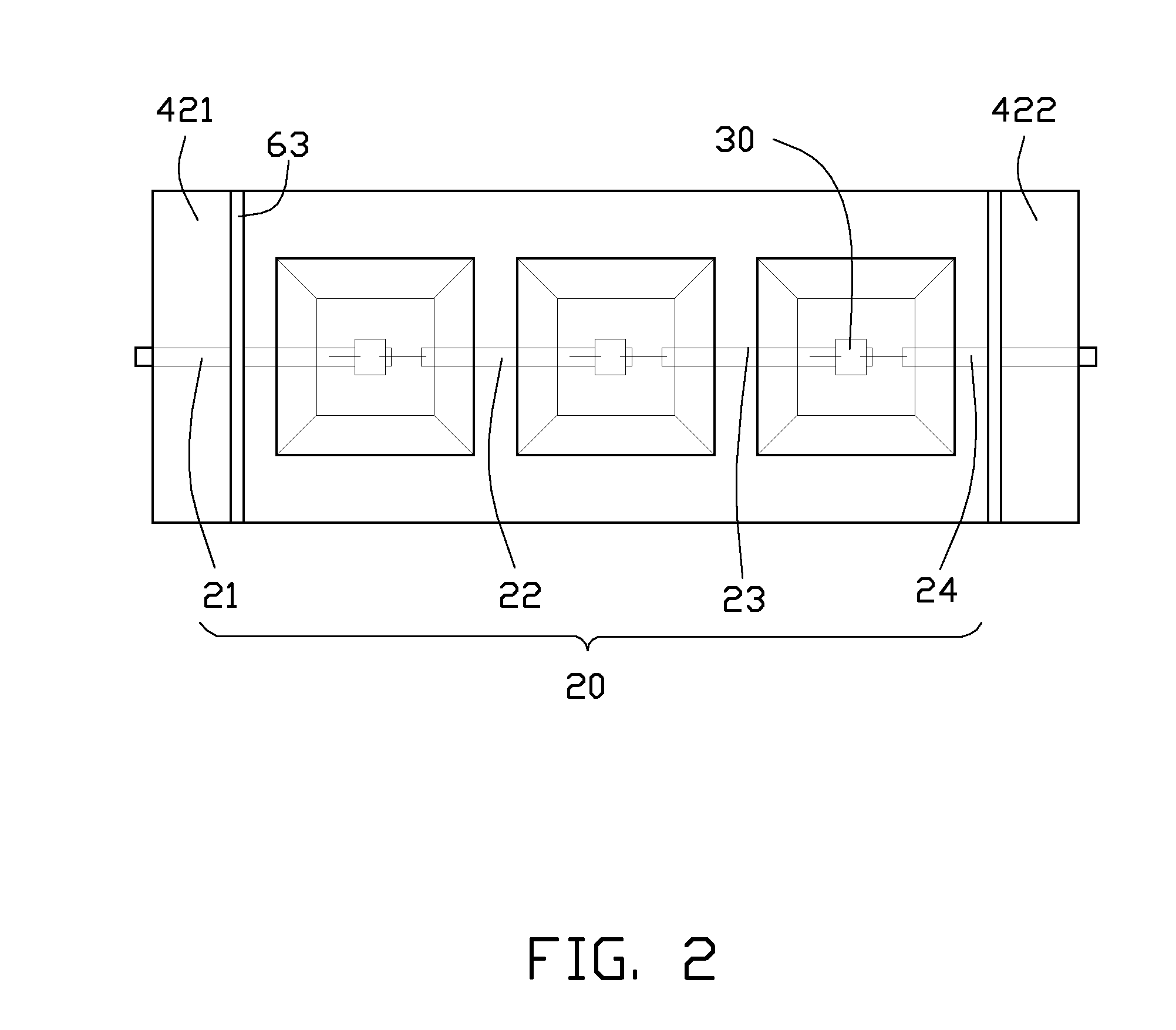
[0014]Referring to FIG. 1, an LED package 100 of a first embodiment includes a first substrate 10, an electrode structure 20, three LED dies 30 fixed on the first substrate 10 and electrically connected to the electrode structure 20, a second substrate 40 attached on the first substrate 10, an encapsulation 50 received in the second substrate 40 and covering the LED dies 30, and a reflective layer 60. The second substrate 40 forms three cup-shaped structures each receiving a corresponding LED die 30 therein. It should be understood that the number of the LED dies 30 is not limited to be three. The first and second substrates 10, 40 are combined together as a substrate (not labeled) with the electrode structure 20 embedded within the substrate.

[0015]The first substrate 10 can be made of a transparent material, such as glass. In this embodiment, the fi...


PUM


Abstract

An LED package includes a substrate with two opposite lateral bulging portions, an LED die, an electrode structure, and a reflective layer. The substrate includes a first substrate and a second substrate stacked together; the first substrate and the second substrate are transparent; and the substrate includes an emitting surface for emitting light of the LED package. The electrode structure is sandwiched between the first substrate and the second substrate. The LED die is mounted in the substrate and electrically connected to the electrode structure. The reflective layer is formed on an outer surface of the substrate except the emitting surface and the bulging portions. The disclosure also provides a method for manufacturing such an LED package.

Description

BACKGROUND[0001]1. Technical Field[0002]The present disclosure generally relates to light emitting diode (LED) packages and method for making the same.[0003]2. Description of Related Art[0004]Generally, an LED package includes a substrate, electrodes formed on the substrate, and an LED die arranged on the substrate and electrically connected to the electrodes. A receiving cavity is usually defined by a cup on the substrate to receive the LED die therein. Generally, a reflective layer is formed on an inner surface of the cup defining the receiving cavity for reflecting out light of the LED die, thereby increasing the luminous efficiency of the LED package.[0005]However, due to that the reflective layer being merely formed in the receiving cavity, the substrate does reflect light as a supplementary means for light reflection. Thus, the luminous efficiency of the LED package is still not satisfactorily high. Furthermore, the process of forming a reflective layer on the inner surface of...

Claims


Application Information

Patent Timeline
IPC IPC(8): H01L33/60H01L33/52H01L33/08
CPCH01L25/0753H01L33/46H01L33/486H01L2224/48091H01L2224/48247H01L2924/00014
Inventor HU, PI-CHIANGHSU, SHIH-YUAN
Owner ADVANCED OPTOELECTRONICS TECH
Features
  • Generate Ideas
  • Intellectual Property
  • Life Sciences
  • Materials
  • Tech Scout
  • Unparalleled Data Quality
  • Higher Quality Content
  • 60% Fewer Hallucinations
Learn More