Optical modulator including liquid crystal, driving method thereof, and optical device using the same

a technology of optical modulator and liquid crystal, which is applied in the direction of instruments, computing, electric digital data processing, etc., can solve problems such as display faults, and achieve the effects of improving the diffraction efficiency of the optical modulation device, easy control of the in-plane rotation angle, and simplifying the process of manufacturing an optical modulation device including liquid crystal

Inactive Publication Date: 2016-02-25
SAMSUNG DISPLAY CO LTD
View PDF6 Cites 8 Cited by
  • Summary
  • Abstract
  • Description
  • Claims
  • Application Information

AI Technical Summary

Benefits of technology

[0033]According to an embodiments of the present invention, the optical phase of outputted light is modulated by easily controlling the in-plane rotation angle of the liquid crystal molecule in the optical modulation device including liquid crystal. Also, the process for manufacturing an optical modulation device including liquid crystal is simplified and a diffraction efficiency of the optical modulation device is increased. Further, the optical modulation device including liquid crystal is manufactured to be widely applicable, such that it can function as a lens, a diffraction lattice, or a prism such that it is usable with various kinds of optical devices.

Problems solved by technology

When the alignment must be finely distinguished and processed, it is difficult to uniformly perform the alignment process, such as a rubbing process, which may cause display faults when used in the display device.

Method used


Image

  • Optical modulator including liquid crystal, driving method thereof, and optical device using the same
  • Optical modulator including liquid crystal, driving method thereof, and optical device using the same
  • Optical modulator including liquid crystal, driving method thereof, and optical device using the same

Examples


Embodiment Construction

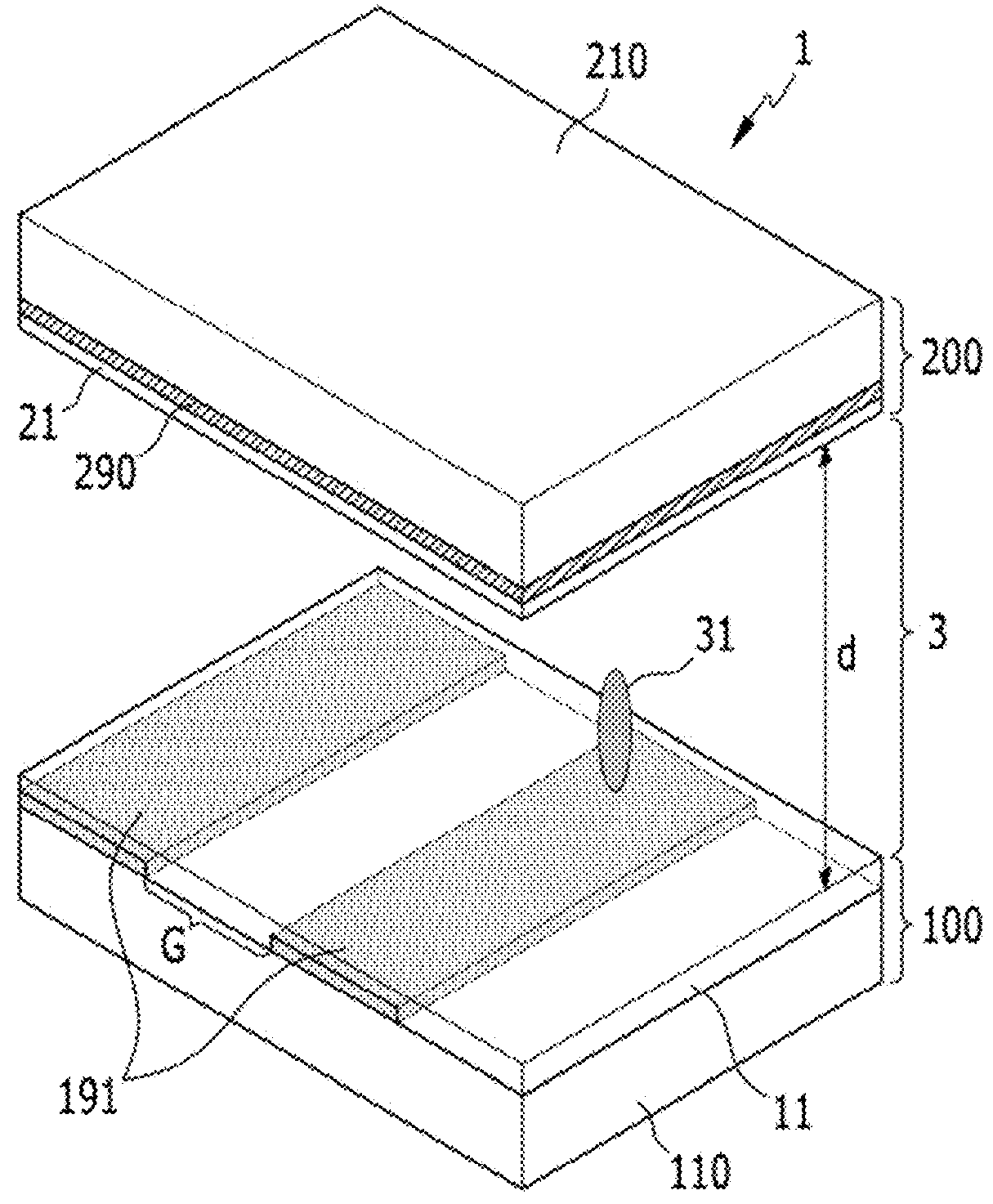
[0065]The present invention will be described more fully hereinafter with reference to the accompanying drawings in which exemplary embodiments of the invention are shown. As those skilled in the art would realize, the described embodiments may be modified in various different ways, all without departing from the spirit or scope of the present invention.

[0066]In the drawings, the thickness of layers, films, panels, regions, etc. may be exaggerated for clarity. Like reference numerals designate like elements throughout the specification. It will be understood that when an element, such as a layer, film, region, or substrate, is referred to as being “on” another element, it can be directly on the other element or intervening elements may also be present. When an element is referred to as being “directly on” another element, there are no intervening elements present.

[0067]Further, the use of “may” when describing embodiments of the present invention relates to “one or more embodiments ...


PUM

PropertyMeasurementUnit
azimuthal angleaaaaaaaaaa
voltageaaaaaaaaaa

Abstract

An optical modulation device or an optical device including the same includes: a first plate and a second plate facing the first plate; and a liquid crystal layer between the first plate and the second plate and including a plurality of liquid crystal molecules, wherein the first plate includes a plurality of first electrodes and a first aligner, the second plate includes at least one second electrode and a second aligner, and an alignment direction of the first aligner is substantially parallel to an alignment direction of the second aligner and wherein portions of the first plate, the second plate, and the liquid crystal layer between the first and second plates are individual units.

Description

CROSS-REFERENCE TO RELATED APPLICATION[0001]This application claims priority to and the benefit of Korean Patent Application No. 10-2014-0110867, filed in the Korean Intellectual Property Office on Aug. 25, 2014, the entire content of which is incorporated herein by reference.BACKGROUND[0002]1. Field[0003]The following description relates to an optical modulation device, a driving method thereof, and an optical device using the same. More particularly, the present invention relates to an optical modulation device using liquid crystal, a driving method thereof, and an optical device using the same.[0004]2. Description of the Related Art[0005]Recently, optical devices (e.g., display devices) using an optical modulation device for modulating an optical characteristic of the optical devices have been widely developed. For example, optical display devices for displaying three-dimensional (3D) images have been paid much attention, and they can include and / or use an optical modulation devi...

Claims


Application Information

Patent Timeline
Patent Type & Authority Applications(United States)
IPC IPC(8): G02F1/137G02F1/1337G02F1/1343G09G3/36
CPCG02F1/137G02F1/134336G09G2300/0426G09G3/3696G02F1/1337G02B5/1828G02F1/292G02F1/13373G02F1/133742G02F1/134381G02B30/27
Inventor OH, SOO HEEPARK, YOON KYUNGJUNG, KYUNG HOJEONG, SEUNG JUNBAEK, MOON JUNGSEO, HYUN SEUNG
Owner SAMSUNG DISPLAY CO LTD
Why Eureka
Try Eureka