Flexible thin film transistor substrate and flexible organic light emitting display device

Active Publication Date: 2016-04-28
LG DISPLAY CO LTD
View PDF30 Cites 70 Cited by
  • Summary
  • Abstract
  • Description
  • Claims
  • Application Information

AI Technical Summary

Benefits of technology

[0029]According to another exemplary embodiment of the present disclosure, there is provided a flexible organic light emitting display device including a flexible substrate, an inorganic insulation layer, an organic insulation layer, and an organic light emitting element. A thin film transistor is disposed on the flexible substrate. The inorganic insulation layer is disposed on the flexible substrate. The organic

Problems solved by technology

However, when the flexible organic light emitting display device is repetitively bent or folded, tension is applied to the inorganic insulation layer and the organic insulation layer included in the flexible organic light emitting display device.
As a result, a crack may be generated in the inorganic insulation layer or the organic insulation layer.
As a result, performance of the organic light emission layer or the active layer may deteriorate.
When a crack between the active layer of the thin film transistor and the inorganic insulation layer occurs and a slip phenomenon occurs where the active layer slips over the inorganic insulation layer due to breaking bonding there between are genera

Method used


Image

  • Flexible thin film transistor substrate and flexible organic light emitting display device
  • Flexible thin film transistor substrate and flexible organic light emitting display device
  • Flexible thin film transistor substrate and flexible organic light emitting display device

Examples


Embodiment Construction

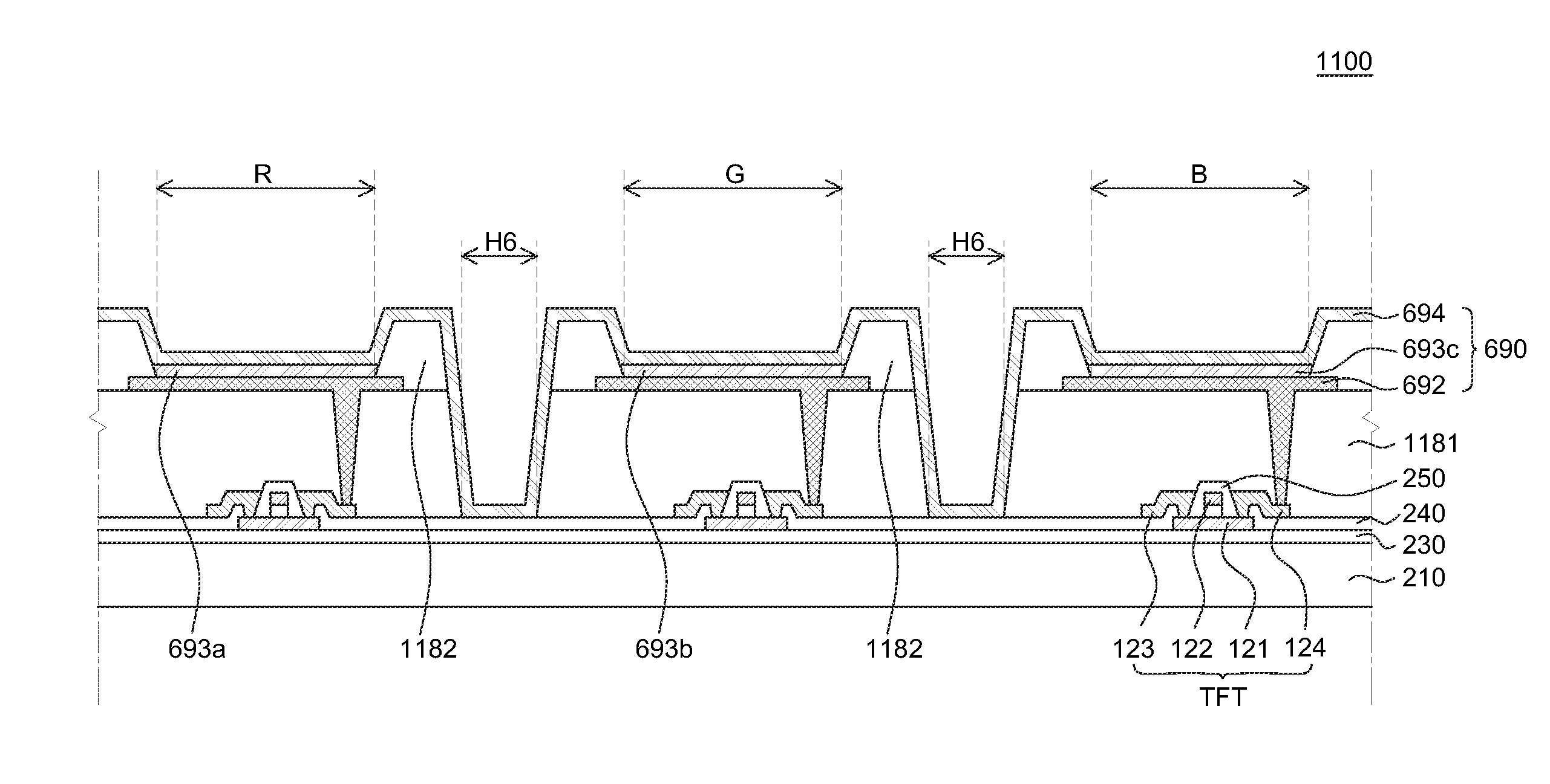
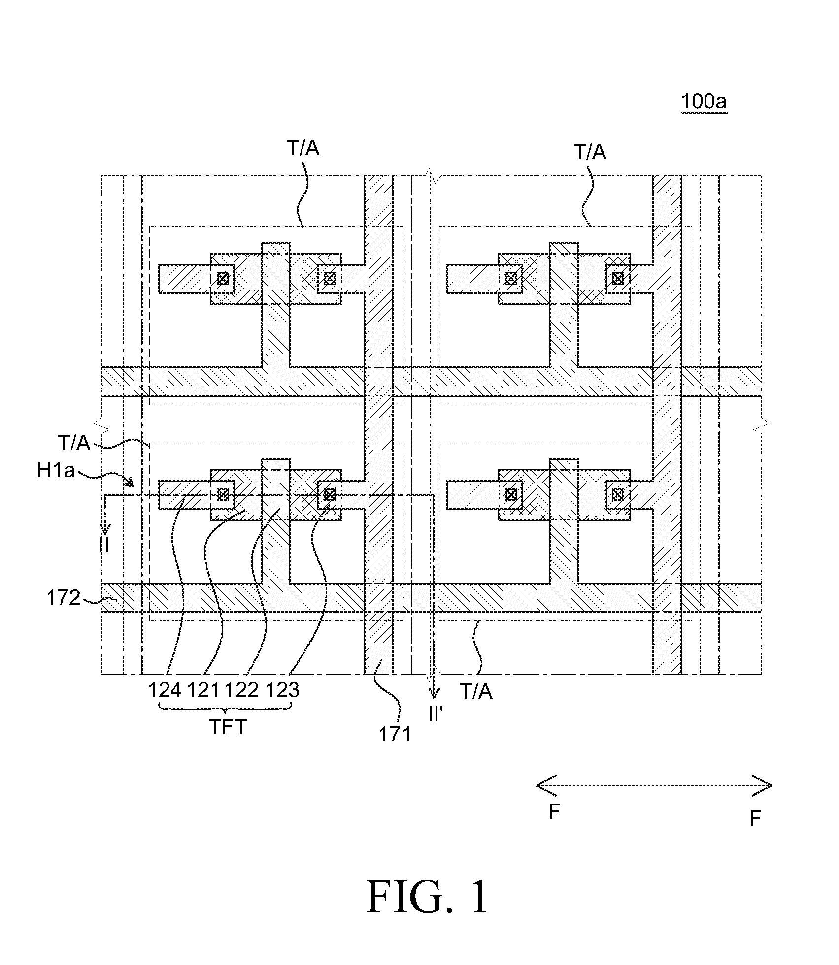
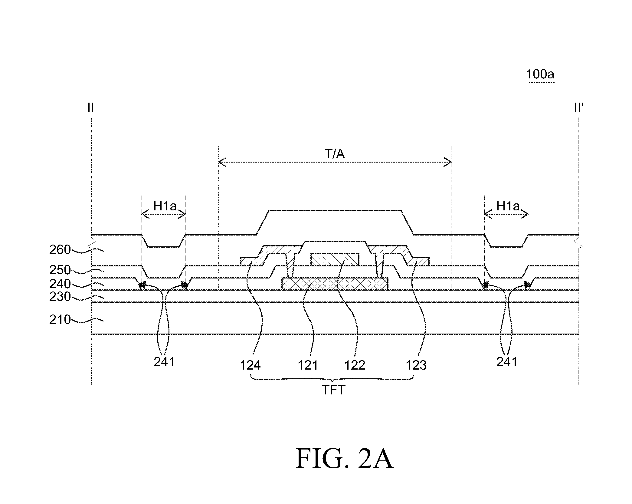
[0062]Various advantages and features of the present disclosure and methods accomplishing thereof will become apparent from the following description of exemplary embodiments with reference to the accompanying drawings. However, the present disclosure is not limited to exemplary embodiment disclosed herein but will be implemented in various forms. The exemplary embodiments are provided by way of example only so that a person of ordinary skilled in the art can fully understand the disclosures of the present disclosure and the scope of the present disclosure. Therefore, the present disclosure will be defined only by the scope of the appended claims.

[0063]The shapes, sizes, ratios, angles, numbers, and the like shown in the accompanying drawings for describing the exemplary embodiments of the present disclosure are merely examples, and the present disclosure is not limited thereto. Like reference numerals generally denote like elements throughout the present specification. Further, in ...


PUM


Abstract

Provided are a flexible thin film transistor substrate and a flexible organic light emitting display device. The flexible thin film transistor substrate includes: a flexible substrate including at least one thin film transistor (TFT) area and having flexibility, an active layer disposed in the TFT area on the flexible substrate, a gate insulation layer disposed on the active layer, a gate electrode overlapping with the active layer on the gate insulation layer, an insulating interlayer disposed on the gate electrode, and a source electrode and a drain electrode disposed on the insulating interlayer and connected with the active layer, respectively. The gate insulation layer or the insulating interlayer includes at least one hole pattern configured to reduce bending stress.

Description

CROSS-REFERENCE TO RELATED APPLICATIONS[0001]This application claims the priority of Korean Patent Application No. 10-2014-0143117 filed on Oct. 22, 2014, and Korean Patent Application No. 10-2014-0154435 filed on Nov. 7, 2014 in the Korean Intellectual Property Office, the disclosure of which are each incorporated herein by reference.BACKGROUND[0002]1. Field[0003]The present disclosure relates to a flexible thin film transistor substrate and a flexible organic light emitting display device, and more particularly, to a flexible thin film transistor substrate and a flexible organic light emitting display device in which performance does not deteriorate in spite of repeated folding.[0004]2. Description of the Related Art[0005]In a display device used in a monitor of a computer, a television (TV), or a mobile phone, an organic light emitting display device self-emitting light, a plasma display panel (PDP) and the like, and a liquid crystal display (LCD) requiring a separate light sourc...

Claims


Application Information

Patent Timeline
IPC IPC(8): H01L27/32H01L51/52H01L27/12
CPCH01L27/3262H01L27/3246H01L27/1218H01L2251/5338H01L27/3276H01L27/3248H01L51/52H01L27/3258H01L29/42384H01L29/78603H01L29/78606H01L27/1248H01L2029/42388H10K59/124H10K59/1213H10K59/131H10K2102/311
Inventor YOUN, SANGCHEONCHOI, NACKBONGCHO, YOONDONG
Owner LG DISPLAY CO LTD
Why Eureka
Try Eureka