In-cell touch liquid crystal display device and method of manufacturing the same

a liquid crystal display device and touch technology, applied in semiconductor devices, instruments, computing, etc., can solve the problems of reducing esd prevention characteristics, complicated manufacturing process, deteriorating yield and touch sensitivity, etc., and achieve the effect of improving touch performance and esd performan

Active Publication Date: 2018-04-05
LG DISPLAY CO LTD
View PDF3 Cites 11 Cited by
  • Summary
  • Abstract
  • Description
  • Claims
  • Application Information

AI Technical Summary

Benefits of technology

[0044]Various embodiments of the present disclosure are directed to an in-cell touch LCD device and a method of manufacturing the same, in which a screen display and a screen touch are implemented through a thin-film transistor substrate having an area larger than that of a color filter substrate, thus improving touch performance and ESD performance.

Problems solved by technology

Also, in the related art, since a transparent conductive layer having a high resistance value, instead of existing ITO, is formed on the color filter substrate, electrostatic spots occur due to the transparent conductive layer, so that ESD prevention characteristics are decreased, and thus a yield and touch sensitivity are deteriorated.
In particular, since the related art technology employs a structure in which a separate metal layer should be formed to form the touch line and in which the data line overlaps the touch line, a process of forming a thick planarization layer between the data line and the touch line should be added so as to reduce the resistance of the touch line, thus causing the entire manufacturing process to be complicated, and increasing manufacturing costs.
Moreover, when the in-cell touch LCD device is manufactured according to the related art, around seven manufacturing masks are required to form at least a gate, a source / drain, a drain contact hole, a pixel electrode, a touch line, a touch line contact hole, and a common electrode, thus increasing the number of panel manufacturing processes and manufacturing costs in proportion to the number of masks.

Method used


Image

  • In-cell touch liquid crystal display device and method of manufacturing the same
  • In-cell touch liquid crystal display device and method of manufacturing the same
  • In-cell touch liquid crystal display device and method of manufacturing the same

Examples


Embodiment Construction

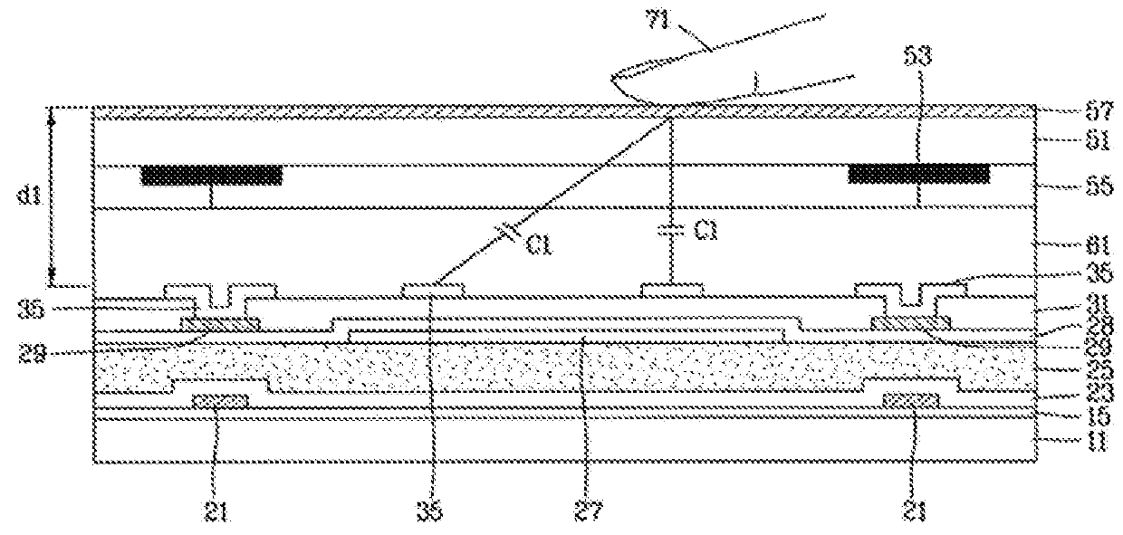
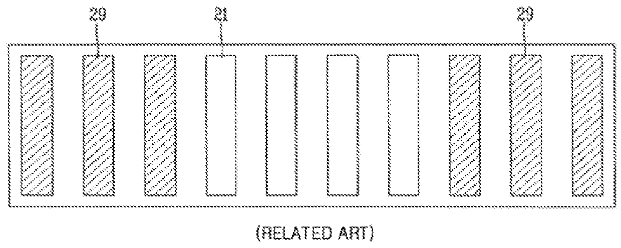
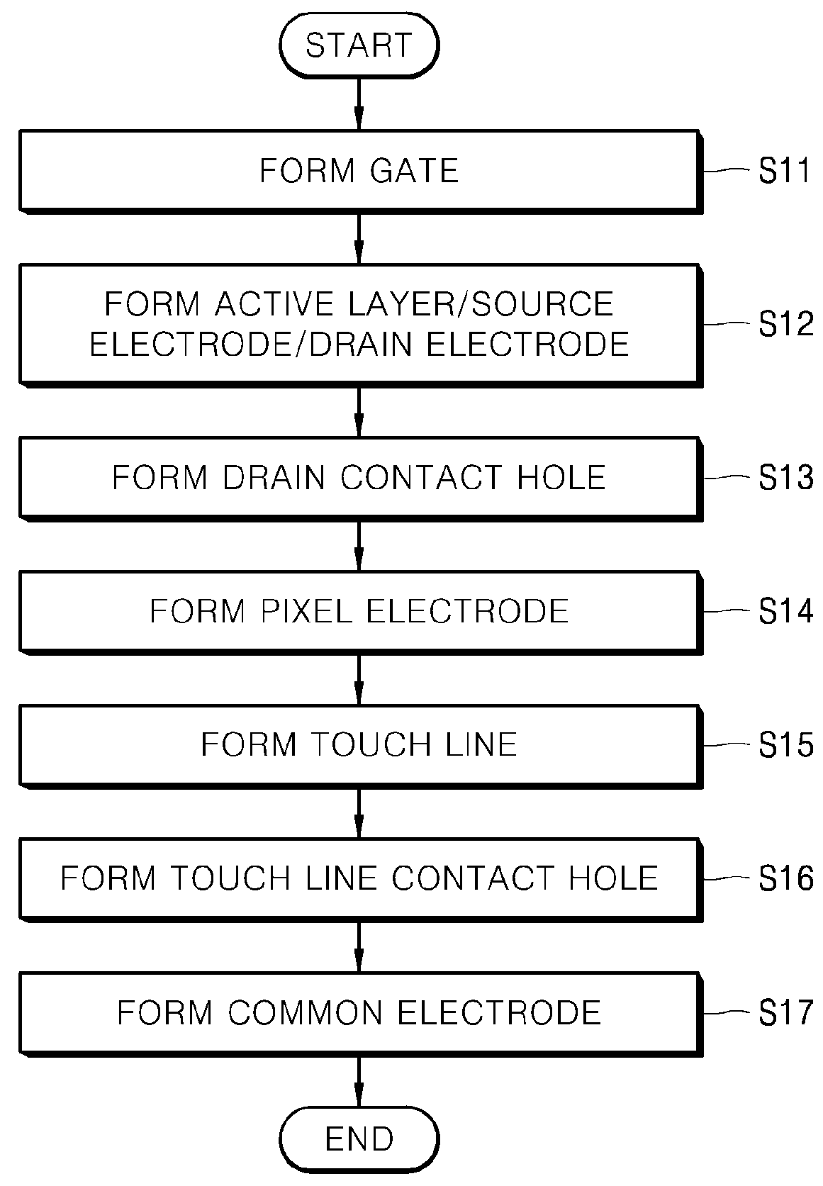
[0081]Hereinafter, embodiments of a borderless Liquid Crystal Display (LCD) device according to the present disclosure will be described in detail with reference to the attached drawings so that those skilled in the art to the present disclosure pertains can easily practice the embodiments.

[0082]The advantages and features of the present disclosure and methods of achieving them will be more clearly understood from the following detailed description taken in conjunction with the accompanying drawings. However, the present disclosure is not limited by embodiments, which will be disclosed later, but may be implemented in different various forms. The embodiments of the present disclosure are intended to fully describe the present disclosure to a person having ordinary knowledge in the art to which the present disclosure pertains, and are defined only by the accompanying claims. It should be noted that the same reference numerals are used to designate the same or similar elements through...


PUM

PropertyMeasurementUnit
areaaaaaaaaaaa
transparentaaaaaaaaaa
transparent conductiveaaaaaaaaaa

Abstract

An in-cell touch LCD device and a method of manufacturing the same are discussed. The in-cell touch LCD device may implement a screen display and a screen touch through a thin-film transistor substrate, which has an area larger than that of a color filter substrate, thus improving touch performance and ESD performance and simplifying a manufacturing process and reducing manufacturing costs.

Description

CROSS-REFERENCE TO RELATED APPLICATION[0001]This application claims the priority benefit of Korean Patent Application No. 10-2016-0126898, filed on Sep. 30, 2016, in the Korean Intellectual Property Office, all of which is fully incorporated by reference into the present application.BACKGROUND1. Technical Field[0002]The present disclosure relates to a liquid crystal display device, and more particularly, to an in-cell touch liquid crystal display device and a method of manufacturing the in-cell touch liquid crystal display device.2. Description of the Related Art[0003]Recently, various types of flat panel display devices that enable the weight and volume of display devices to be reduced have been developed, in view of the disadvantages of Cathode Ray Tubes (CRTs). Examples of such flat panel display devices may include a Liquid Crystal Display (LCD), a Field Emission Display (FED), a Plasma Display Panel (PDP), an electroluminescence (EL) Device, etc.[0004]Since these flat-panel dis...

Claims


Application Information

Patent Timeline
Patent Type & Authority Applications(United States)
IPC IPC(8): G02F1/1333G02F1/1343G06F3/041G02F1/1335H01L27/12
CPCG02F1/13338G02F1/1343G06F3/0412G02F1/133514H01L27/1214G06F2203/04103G06F3/045G06F3/047G06F3/0445G06F2203/04107G06F1/1637G06F1/1643G06F1/1626G06F3/0443G06F3/044G02F1/1362G02F1/1335G02F1/133308G02F2202/22
Inventor PYO, JONGSANGSHIN, CHULSANGCHA, JEHEON
Owner LG DISPLAY CO LTD
Why Eureka
Try Eureka