Method, flash memory controller, memory device for accessing flash memory

a flash memory and controller technology, applied in the field of flash memory, can solve the problems of data errors also occurring at floating gate transistors on the other word lines, etc., and achieve the effect of less buffer memory spa

Active Publication Date: 2018-09-13
SILICON MOTION INC (TW)
View PDF4 Cites 7 Cited by
  • Summary
  • Abstract
  • Description
  • Claims
  • Application Information

AI Technical Summary

Benefits of technology

[0004]Therefore one of the objectives of the present invention is to provide a method for accessing a flash memory module, a corresponding flash memory controller, and a memory device. The method employs RAID-like (Redundant Array of Independent Disks-like) error correction mechanism without occupying more flash memory space and merely with less buffer memory space, to solve the problems mentioned above.

Problems solved by technology

For a conventional 3D NAND-type flash memory, since the manufacture structure becomes totally different and positions of floating gates are changed, it becomes more complicated for data writing and reading compared to a traditional 2D NAND-type flash memory, and thus some serious problems arise.
This inevitably causes that data errors also occur at floating gate transistors on the other word lines within a word line set if program fail occurs at floating gate transistors on one word line of the same word line set.
In addition, data errors also occur at floating gate transistors on the other word lines within a word line set if one word line is open or two word lines are short for the same word line set.

Method used


Image

  • Method, flash memory controller, memory device for accessing flash memory
  • Method, flash memory controller, memory device for accessing flash memory
  • Method, flash memory controller, memory device for accessing flash memory

Examples


Embodiment Construction

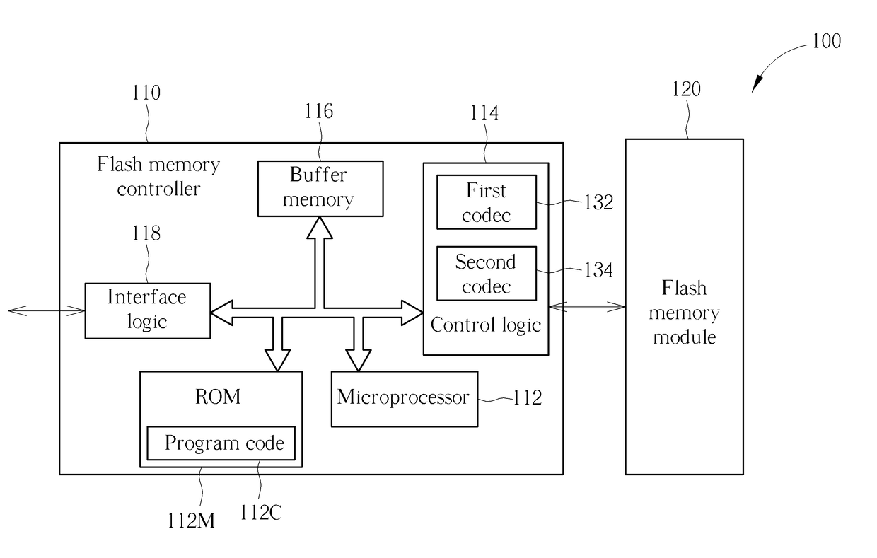
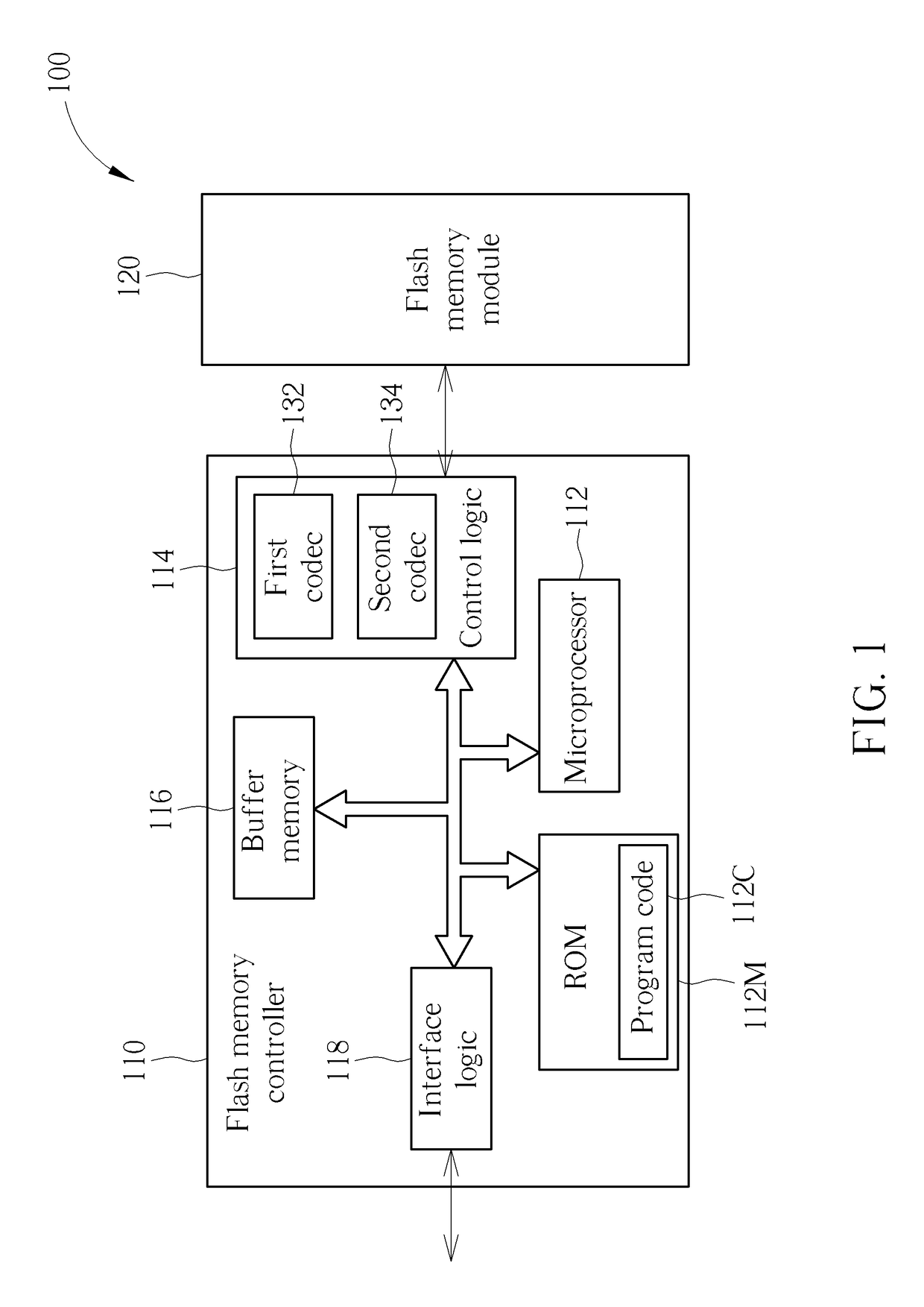
[0023]Please refer to FIG. 1, which is a diagram of a memory device 100 according to an embodiment of the present invention. In the embodiment, the memory device 100 can be a portable memory device such as a memory card conforming to the standards of SD / NMC, CF, MS, and XD. The memory device 100 comprises a flash memory module 120 and a flash memory controller 110. The flash memory controller 110 is used for accessing the flash memory module 120. In the embodiment, the flash memory controller 110 comprises a microprocessor 112, read-only memory (ROM) 112M, control logic 114, buffer memory 116, and an interface logic 118. The read-only memory is used for storing program codes 112C. The microprocessor 112 is used for executing the program codes 112C to control the access of flash memory module 120. In other embodiments, the buffer memory 116 can be configured outside of the controller 110, and is implemented with a storage space allocated by a dynamic random access memory.

[0024]Typica...


PUM


Abstract

A method for accessing a flash memory module is provided. The flash memory module is a 3D flash memory module including a plurality of flash memory chips, each flash memory chip includes a plurality of blocks, each block includes a plurality of pages, and the method includes: configuring the flash memory chips to set at least one super block of the flash memory chips; and allocating a buffer memory space to store a plurality of temporary parities generated when data is written into the at least one first super block.

Description

CROSS REFERENCE TO RELATED APPLICATIONS[0001]This division application claims the benefits of U.S. application Ser. No. 15 / 497,217 filed on 2017 / 04 / 26 which claims the benefits of corresponding Foreign Application No. TW 106100010 filed on 2017 Jan. 3 and claims priority of U.S. provisional application Ser. No. 62 / 328,025 filed on Apr. 27, 2016 and priority of U.S. provisional application Ser. No. 62 / 328,027 filed on Apr. 27, 2016, which are entirely incorporated herein by reference.BACKGROUND OF THE INVENTION1. Field of the Invention[0002]The present invention relates to a flash memory, and more particularly to a method for accessing a flash memory module, a corresponding flash memory controller, and a memory device.2. Description of the Prior Art[0003]In order to make a flash memory with higher storage density and more capacity, the 3D flash memory manufacture becomes more important, and a variety of 3D NAND-type flash memory manufactures have been developed. For a conventional 3D...

Claims


Application Information

Patent Timeline
Patent Type & Authority Applications(United States)
IPC IPC(8): G06F12/02G06F11/10G06F3/06G11C7/10G11C11/56G11C16/04G11C16/08G11C16/10G11C16/26G11C29/52
CPCG11C16/08G11C29/52G06F3/0679G06F11/1072G06F12/0246G11C11/5642G11C11/5628G11C2211/5641G11C16/0483G11C16/10G11C16/26G11C7/1006G06F3/062G06F3/064G06F3/0644G06F3/0656G06F11/1004G06F12/0882G06F2212/7209G11C29/42
Inventor YANG, TSUNG-CHIEHHSU, HONG-JUNG
Owner SILICON MOTION INC (TW)
Why Eureka
Try Eureka