Liquid crystal device and electronic device

a liquid crystal device and electronic device technology, applied in non-linear optics, instruments, optics, etc., can solve the problems of deteriorating the display performance deteriorating the display quality of the liquid crystal device, and not preventing the hydrophilized layer, so as to reduce the effect of attracting

Inactive Publication Date: 2018-09-20
SEIKO EPSON CORP
View PDF0 Cites 4 Cited by
  • Summary
  • Abstract
  • Description
  • Claims
  • Application Information

AI Technical Summary

Benefits of technology

[0004]However, the formation of the inorganic alignment film and the treatment with the silane coupling agent are performed over the entire surface of the first substrate. Thus, in the liquid crystal device in which the first substrate has the peripheral electrode for trapping the ionic im

Problems solved by technology

This causes ionic impurities mixed during injection of liquid crystal or ionic impurities eluted from the sealing member to concentrate at a corner of the display region, for example, leading to image sticking (smear) or the like that deteriorates the display quality.
Repetition of the photochemical reactio

Method used


Image

  • Liquid crystal device and electronic device
  • Liquid crystal device and electronic device
  • Liquid crystal device and electronic device

Examples


first embodiment

Overall Configuration of Liquid Crystal Device 100

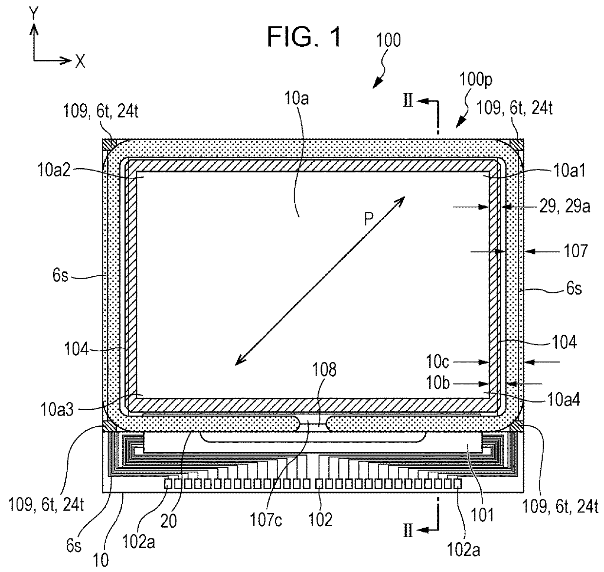
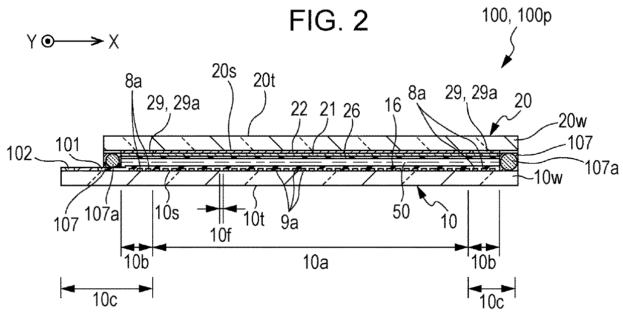
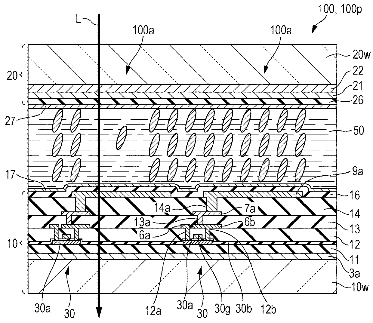
[0031]FIG. 1 is a plan view illustrating a configuration example of a liquid crystal device 100 according to a first embodiment of the invention. FIG. 2 is a cross-sectional view of the liquid crystal device 100 taken along line II-II in FIG. 1. The liquid crystal device 100 illustrated in FIG. 1 and FIG. 2 includes a liquid crystal panel 100p. In the liquid crystal device 100, a first substrate 10 (an element substrate) and a second substrate 20 (a counter substrate) are connected to each other by a sealing member 107 with a predetermined space therebetween. The sealing member 107 has a frame-like shape extending along the outer edge of the second substrate 20. The sealing member 107 is an adhesive formed of a light-curing resin or a thermal curing resin and contains a gap material 107a such as fiberglass, glass beads, or the like so as to maintain a predetermined distance between the first substrate 10 and the second substrate 20. ...

second embodiment

[0057]FIG. 7 is a cross-sectional view schematically illustrating components around the peripheral electrode 8a of a liquid crystal device 100 according to a second embodiment of the invention. The basic components of the second embodiment and third and fourth embodiments described below are the same as those of the first embodiment. Thus, identical reference numerals are used to denote identical components, and the components are not described in detail.

[0058]As illustrated in FIG. 7, in this embodiment, the first substrate 10 has the peripheral electrode 8a in the peripheral region 10b as in the first embodiment. In addition, the organic silane compound layers 17 and 27 are respectively disposed on the surfaces of the first and second alignment films 16 and 26 adjacent to the liquid crystal layer 50. Here, the first alignment film 16 and the organic silane compound layer 17 are disposed over the entire display region 10a, but are not disposed in the region 10d overlapping the peri...

third embodiment

[0060]FIG. 8 is a cross-sectional view schematically illustrating components around the peripheral electrode 8a of a liquid crystal device 100 according to a third embodiment of the invention. As illustrated in FIG. 8, in this embodiment, the first substrate 10 has the peripheral electrode 8a in the peripheral region 10b as in the first embodiment. Furthermore, the organic silane compound layers 17 and 27 are respectively disposed on the surfaces of the first and second alignment films 16 and 26 adjacent to the liquid crystal layer 50. Here, the first alignment film 16 is formed in the display region 10a and the peripheral region 10b, but the organic silane compound layer 17 is formed only in the display region 10a and is not formed in the peripheral region 10b. Thus, although the organic silane compound layer 17 is disposed on the surface of the inorganic alignment film (the first alignment film 16) adjacent to the liquid crystal layer 50, the surface of the first substrate 10 adja...


PUM


Abstract

In a liquid crystal device, a peripheral electrode is disposed in a peripheral region of a first substrate between a display region and a sealing member. Application of a proper voltage between the peripheral electrode and a common electrode causes ionic impurities to stay outside the display region. In the display region, an organic silane compound layer is disposed on a surface of a first alignment film, which is formed of an inorganic alignment film, adjacent to a liquid crystal layer, but the first alignment film and the organic silane compound layer are not formed in a region overlapping the peripheral electrode in plan view. Thus, the surface of the first substrate adjacent to the liquid crystal layer has higher hydrophilicity at the region overlapping the peripheral electrode than at the display region.

Description

BACKGROUND1. Technical Field[0001]The present invention relates to a liquid crystal device including an inorganic alignment film on a substrate, and an electronic device including the liquid crystal device.2. Related Art[0002]A liquid crystal device includes a first substrate having a pixel electrode in a display region, a second substrate having a common electrode facing the pixel electrode, a sealing member connecting the first substrate and the second substrate to each other, and a liquid crystal layer between the first substrate and the second substrate in a region surrounded by the sealing member. In the liquid crystal device, the orientation of liquid crystal molecules is changed when the liquid crystal device is powered on, generating a flow in the liquid crystal layer. This causes ionic impurities mixed during injection of liquid crystal or ionic impurities eluted from the sealing member to concentrate at a corner of the display region, for example, leading to image sticking...

Claims


Application Information

Patent Timeline
IPC IPC(8): G02F1/1337G02F1/1343G02F1/1335G02F1/1339
CPCG02F1/1337G02F1/134309G02F1/133512G02F1/1339G02F1/133719G02F1/133388
Inventor TANAKA, NOBUTAKA
Owner SEIKO EPSON CORP
Why Eureka
Try Eureka