Array substrate and display panel including same

a display panel and substrate technology, applied in non-linear optics, instruments, optics, etc., can solve the problems of display problems and the low and achieve the effect of increasing the opening rate of pixel and transmittan

Inactive Publication Date: 2019-03-21
HKC CORP LTD
View PDF1 Cites 0 Cited by
  • Summary
  • Abstract
  • Description
  • Claims
  • Application Information

AI Technical Summary

Benefits of technology

[0007]To resolve the foregoing technical problem, an objective of this application is to provide a pixel design method, and in particular, an array substrate and a display panel including same, so as to not only effectively resolve a color shift problem, but also effectively improve a viewing angle of a product having a large size and high resolution, thereby increasing transmittance of the product having a large size and high resolution.
[0019]This application may resolve a color shift problem of an LCD panel and increase an opening rate of a pixel and transmittance.

Problems solved by technology

However, in such design, as resolution is increasingly high, a pixel is increasingly small, a space occupied by active switches is increasingly large, and consequently, an opening rate is increasingly low.
However, such an improvement method may cause some display problems.

Method used


Image

  • Array substrate and display panel including same
  • Array substrate and display panel including same
  • Array substrate and display panel including same

Examples


Embodiment Construction

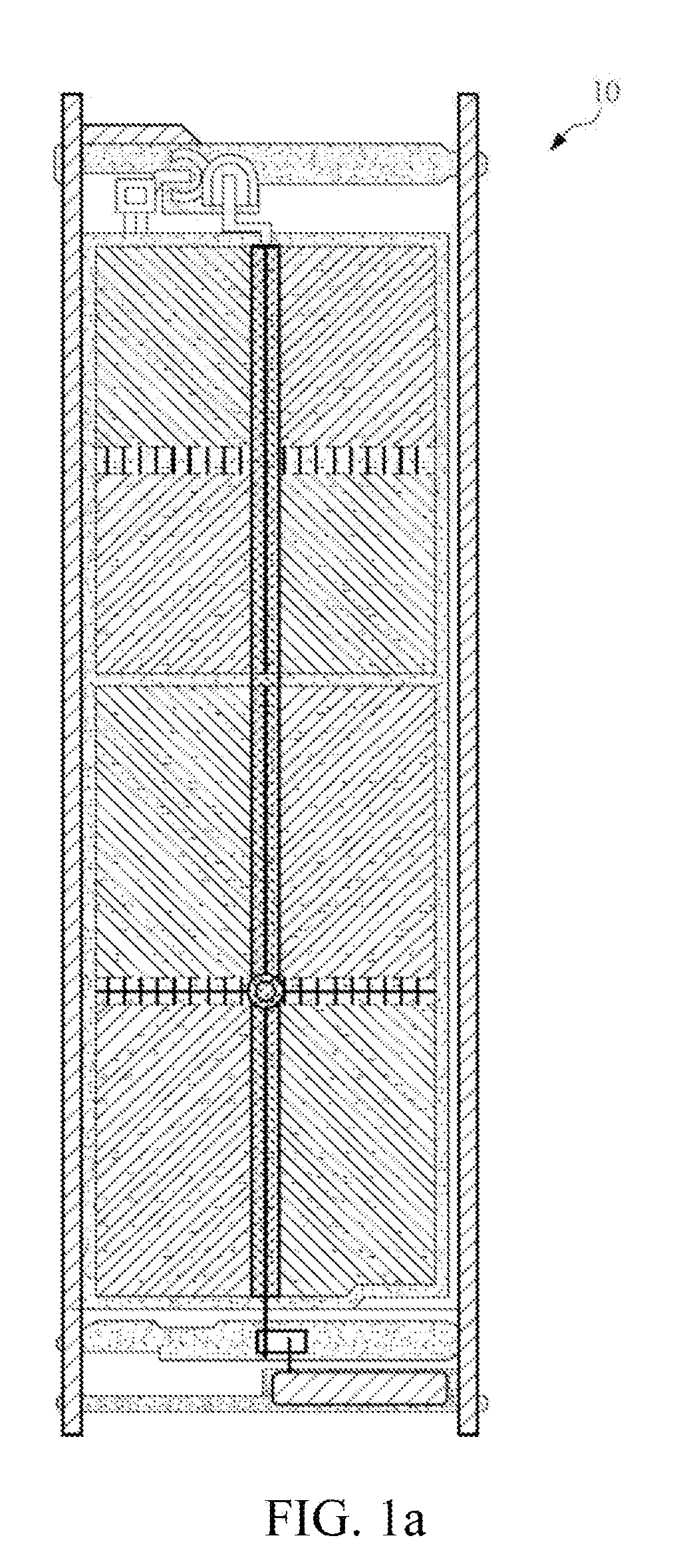
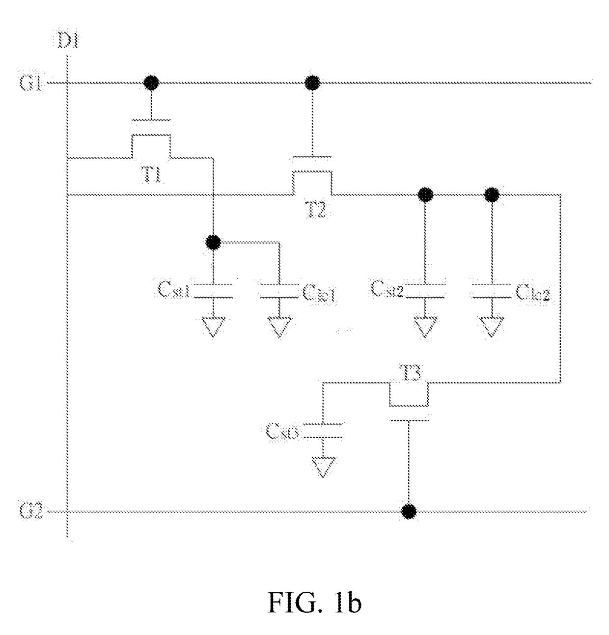
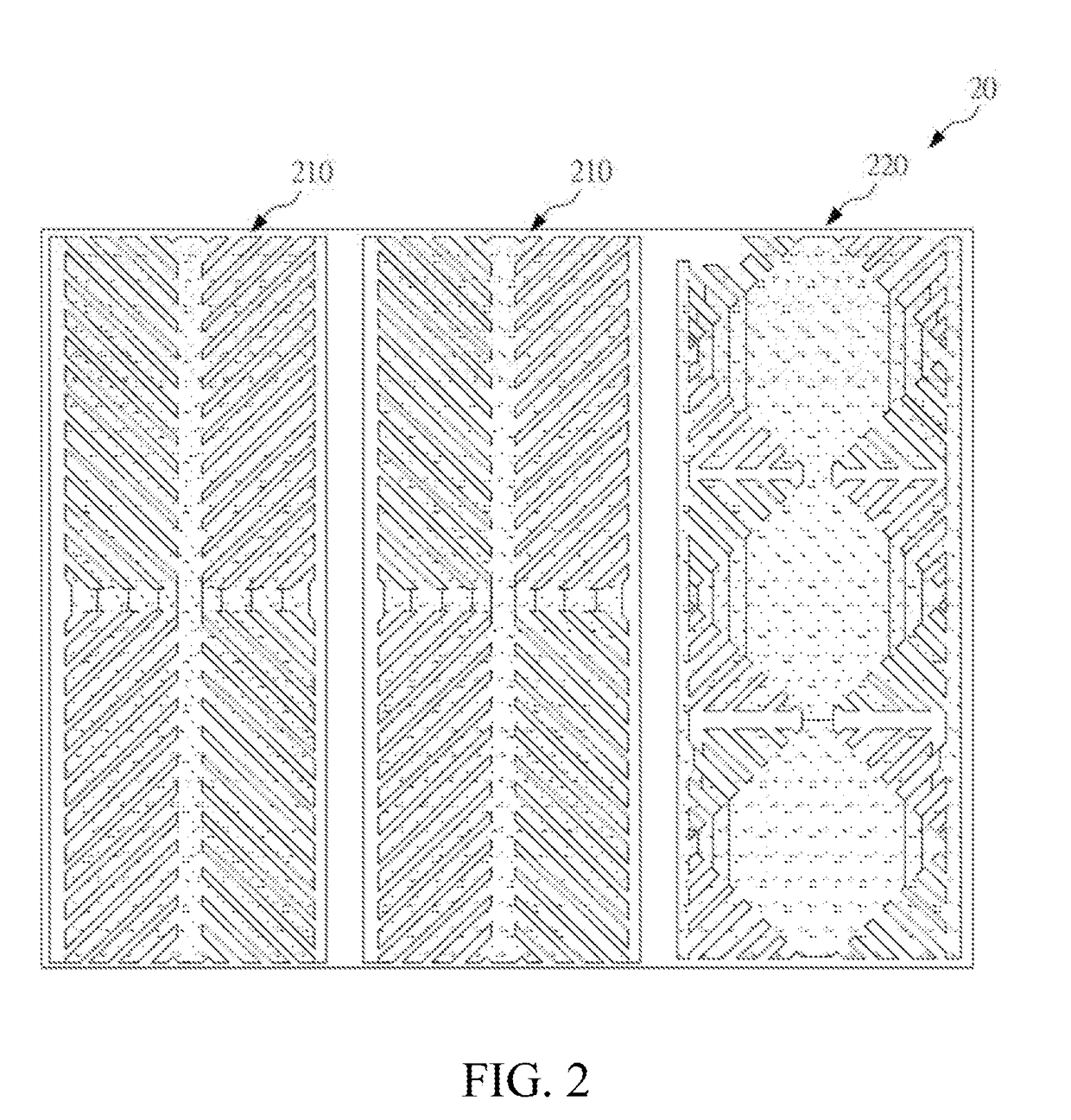
[0029]The following embodiments are described with reference to the accompanying drawings, and are used to exemplify particular embodiments for implementation of this application. Terms about directions mentioned in this application, such as “on”, “below”, “front”, “back”, “left”, “right”, “in”, “out”, and “side face”, merely refer to directions in the accompanying drawings. Therefore, the used terms about directions are used to describe and understand this application, and are not intended to limit this application.

[0030]The accompanying drawings and the description are considered to be essentially exemplary, rather than limitative. In the figures, units with similar structures are represented by using the same reference number. In addition, for understanding and ease of description, the size and the thickness of each component shown in the accompanying drawings are arbitrarily shown, but this application is not limited thereto.

[0031]In the accompanying drawings, for clarity, thick...


PUM

PropertyMeasurementUnit
colorsaaaaaaaaaa
electricallyaaaaaaaaaa
wide-angle viewaaaaaaaaaa

Abstract

An array substrate includes: a substrate, having a display region and a wiring region; at least one active switch, disposed on the substrate; a plurality of scanning lines and a plurality of data lines, disposed on the substrate, where the scanning lines are electrically connected to a control end of the active switch, and the data lines are electrically connected to an input end of the active switch; and a plurality of pixels, disposed on the display region and electrically connected to an output end of the active switch, where: the pixels include a VA pixel and at least one polymer-stabilized VA pixel, where: the polymer-stabilized VA pixel is a blue pixel; and a pixel electrode of the VA pixel and a pixel electrode of the polymer-stabilized VA pixel are separately electrically coupled to the substrate.

Description

BACKGROUNDTechnical Field[0001]This application relates to a pixel design method, and in particular, to an array substrate and a display panel including same.Related Art[0002]A liquid crystal display (LCD) panel usually includes a color filter (CF) substrate, an active switch array substrate (thin film transistor array substrate, TFT Array Substrate), and a liquid crystal layer disposed between the two substrates. A working principle of the LCD is controlling rotation of liquid crystal molecules of the liquid crystal layer by applying a driving voltage to two glass substrates, so as to refract light from a backlight module to generate an image. According to different liquid crystal orientation manners, LCD panels in the current mainstream market may be classified into the following types: a vertical alignment (VA) type, a twisted nematic (TN) or a super twisted nematic (STN) type, an in-plane switching (IPS) type, and a fringe field switching (FFS) type.[0003]LCDs of a VA mode inclu...

Claims


Application Information

Patent Timeline
Patent Type & Authority Applications(United States)
IPC IPC(8): G02F1/1343G02F1/1362G02F1/1337G02F1/1368G02F1/1335
CPCG02F1/134309G02F1/136286G02F1/133703G02F1/1368G02F1/133514G02F2001/134354G02F1/13624G02F1/134354
Inventor HUANG, BEIZHOU
Owner HKC CORP LTD
Why Eureka
Try Eureka