Touch sensor integrated display device with multiple planarization layers

a display device and touch sensor technology, applied in the field of display devices, can solve the problems of reducing compromising the display quality, and affecting the fine-tuning of the touch-sensing and display functionalities, so as to reduce the size of the inactive area at the side of the panel, reduce the delay of rc, and increase the capacitance of the pixel

Active Publication Date: 2016-10-06
LG DISPLAY CO LTD
View PDF4 Cites 23 Cited by
  • Summary
  • Abstract
  • Description
  • Claims
  • Application Information

AI Technical Summary

Benefits of technology

[0017]In the embodiments disclosed in the present disclosure, the common signal lines are arranged parallel to the data line and routed directly towards the inactive area across the active area. By routing the common signal lines directly across the active area, the size of the inactive area at the side of the panel can be reduced. Further, the thickness of the passivation layer between the pixel electrode PXL and the common electrode blocks can be kept minimal to increase the capacitance of the pixel. Since, the common signal lines can be spaced farther away from the common electrode blocks, they can be provided with a desired thickness to decrease RC delays during touch-sensing period. In addition, there is no fringe field generated between the common electrode blocks and the common signal lines as the common electrode blocks positioned above the common signal lines. This effectively solves the light leakage problem caused by having the common signal lines in the same layer as the pixel electrode PXL.

Problems solved by technology

However, placing a separate touch panel on the display panel adds thickness and weight to the display device.
However, integrating touch sensor components within the display pixel often leads to compromises in the display qualities.
However, fine-tuning of the touch-sensing and the display functionalities is especially challenging in an in-plane-switching (IPS) mode and a fringe-field-switching (FFS) mode LCD displays as the electrodes for controlling the orientation of the liquid crystal molecules are provided on one side of the liquid crystal layer.

Method used


Image

  • Touch sensor integrated display device with multiple planarization layers
  • Touch sensor integrated display device with multiple planarization layers
  • Touch sensor integrated display device with multiple planarization layers

Examples


Embodiment Construction

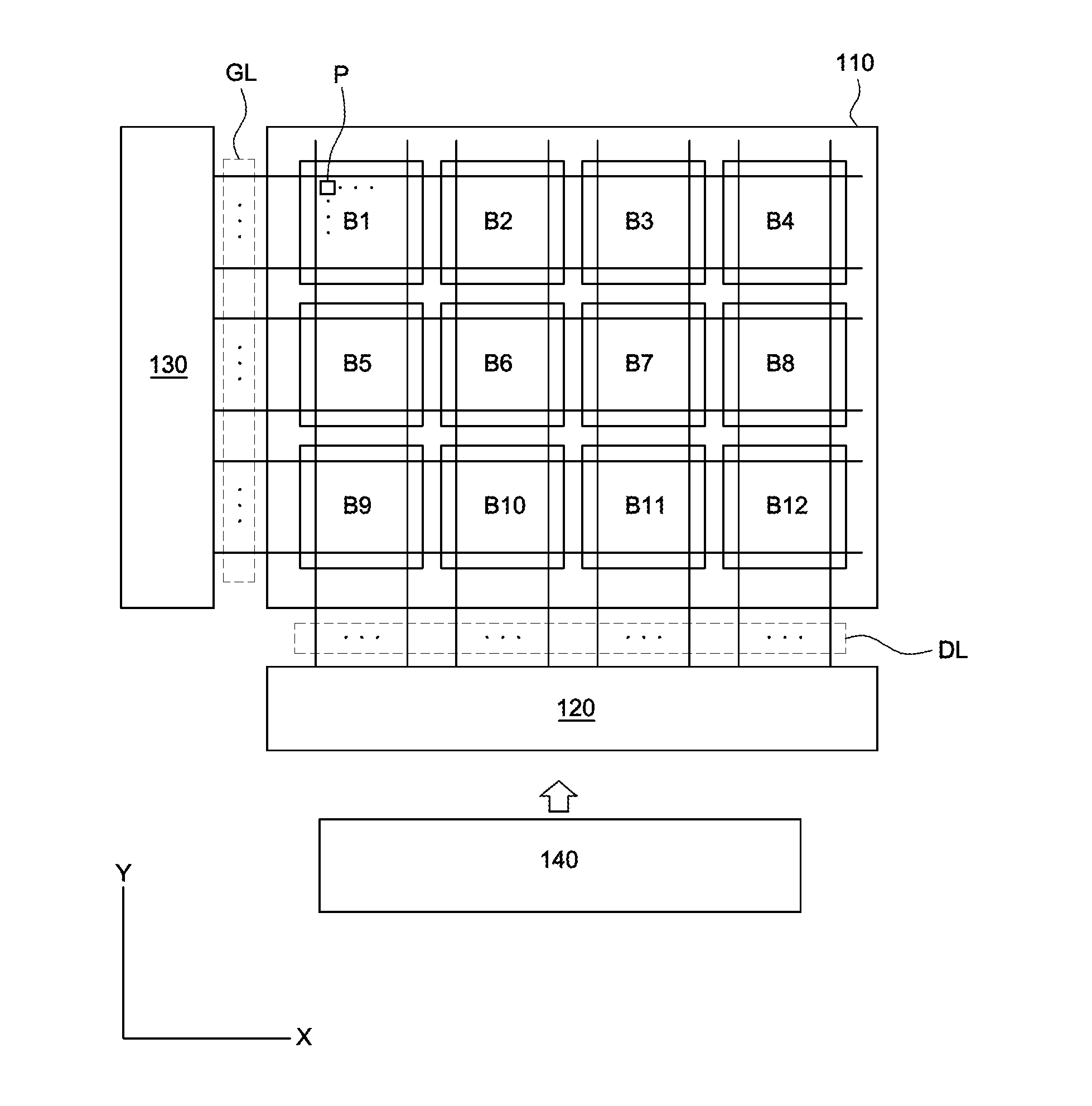
[0029]Reference will now be made in detail to the exemplary embodiments of the present invention, examples of which are illustrated in the accompanying drawings. Wherever possible, the same reference numbers will be used throughout the drawings to refer to the same or like parts.

[0030]The following description includes embodiments described in the context of LCDs, in particular the In-Plane-Switching (IPS) mode LCD and the Fringe-Field-Switching (FFS) mode LCD, in which the common electrodes and the pixel electrodes of the pixels are arranged on one of the substrates that enclose the liquid crystal layer.

[0031]Example embodiments may be described herein with reference to a Cartesian coordinate system in which the x-direction and the y-direction can be equated to the horizontal direction and the vertical direction, respectively. However, one skilled in the art will understand that reference to a particular coordinate system is simply for the purpose of clarity, and does not limit the...


PUM


Abstract

A touch sensor integrated display device includes a plurality of common electrode blocks serving as touch-sensing regions and/or touch-driving regions. Conductive lines connected to the common electrode blocks are placed under the common electrode blocks and the pixel electrodes of the pixels, and they are routed across the active area, directly toward an inactive area where drive-integrated circuits are located. The conductive lines are positioned under one or more planarization layers, and are connected to the corresponding common electrode blocks via one or more contact holes.

Description

BACKGROUND OF THE INVENTION[0001]1. Field of the Invention[0002]The present disclosure generally relates to a display device, and more particularly to a display device configured for advanced mutual capacitance touch-sensing and a method for manufacturing the same.[0003]2. Description of the Related Art[0004]With ease of use and versatility in operation, touch sensor have been one of the most popular user input mechanism in a variety of electronic devices. In particular, touch screens allow a user to interact with a device by touching the screen using a finger, stylus or other object at a location often dictated by a user interface (UI) displayed on flat panel displays, such as liquid crystal displays (LCDs) or organic light emitting diode (OLED) displays.[0005]Conventionally, a substrate with a matrix of touch-driving lines and touch-sensing lines can be overlaid across a display to provide touch-sensing functionality. However, placing a separate touch panel on the display panel ad...

Claims


Application Information

Patent Timeline
Patent Type & Authority Applications(United States)
IPC IPC(8): G06F3/041G06F3/044
CPCG06F3/044G06F3/0412G06F3/04166G06F3/0446
Inventor KIM, BYOUNGWOO
Owner LG DISPLAY CO LTD
Why Eureka
Try Eureka