Organic electroluminescent device and method for producing same

Active Publication Date: 2021-02-25
SAKAI DISPLAY PROD
View PDF0 Cites 0 Cited by
  • Summary
  • Abstract
  • Description
  • Claims
  • Application Information

AI Technical Summary

Benefits of technology

[0033]An embodiment, of the present invention provides an organic EL device including a thin film encapsulation structure that includes a relatively thin organic barrier layer, by which the mass-productivity and the moisture-resistance r

Problems solved by technology

An OLED (especially, an organic light emitting layer and a cathode electrode material) is easily influenced by moisture to be deteriorated and to cause display unevenness.
However, such a thick organic barrier layer involves a problem of limiting the bendability

Method used


Image

  • Organic electroluminescent device and method for producing same
  • Organic electroluminescent device and method for producing same
  • Organic electroluminescent device and method for producing same

Examples


Example

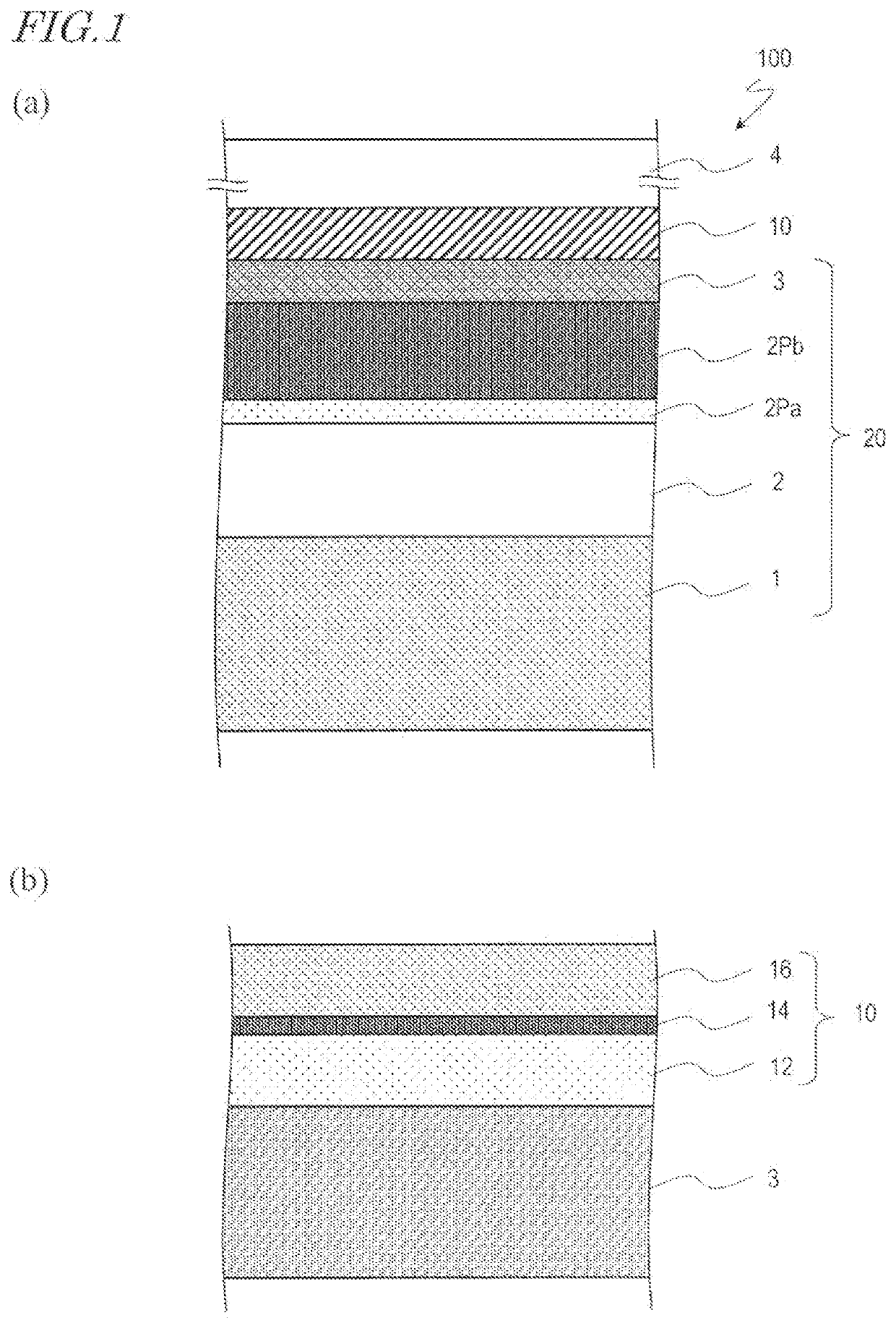
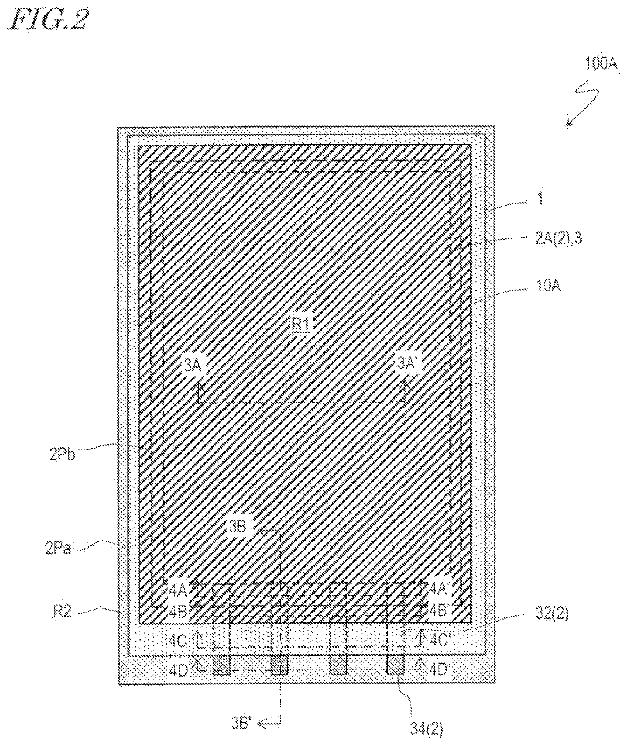
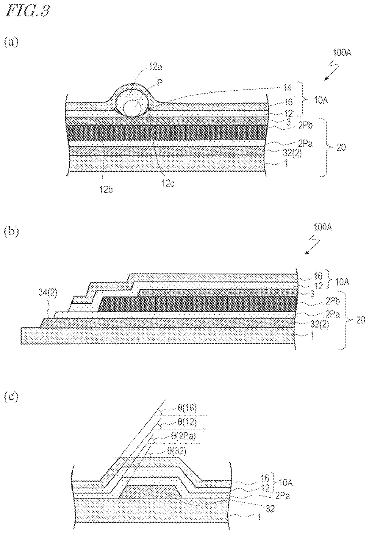
[0049]Hereinafter, an OLED display device and a method for producing the same according to an embodiment of the present invention will be described with reference to the drawings. In the following, an OLED display device including a flexible substrate will be described as an example. Nonetheless, embodiments of the present invention are not limited to being directed to an organic EL display device, but may be directed to another organic EL device such as an organic EL illumination device or the like. Embodiments of the present invention are not limited to the embodiments described below as examples.

[0050]First, with reference to FIG. 1(a) and FIG. 1(b), a basic structure of an OLED display device 100 according to an embodiment of the present invention will be described. FIG. 1(a) is a schematic partial cross-sectional view of an active region of the OLED display device 100 according to an embodiment of the present invention. FIG. 1(b) is a partial cross-sectional view of a TFE struc...


PUM


Abstract

An organic EL device (100D) according to an embodiment of the present invention has: a substrate (1); a drive circuit layer (2) having a plurality or TFTs formed on the substrate; interlayer insulation layers (2Pa, 2Pb) formed on the drive circuit layer; an organic EL element layer (3) formed on the interlayer insulation layers; and a thin-film sealing structure (10DE) formed so as to cover the organic EL element layer. The interlayer insulation layers have contact holes (CH1, CH2). Contact parts (C1, C2) that connect the drive circuit layer and the organic EL element layer are formed inside the contact holes. The surface (2Pb_Sb) of the interlayer insulation layers and the surface (C_Sb) of the contact parts are flush, and the arithmetic average roughness Ra of the surfaces are 50 nm or less.

Description

TECHNICAL FIELD[0001]The present invention relates to an organic EL device (e.g., organic EL display device and organic EL illumination device) and a method for producing the same.BACKGROUND ART[0002]Organic EL (Electroluminescent) display devices start being put into practical use. One feature of an organic EL display device is flexibility thereof. Such an organic EL display device includes, in each of pixels, at least one organic EL element (Organic Light Emitting Diode: OLED) and at least one TFT (Thin Film Transistor) controlling an electric current to be supplied to each of the at least one OLED. Hereinafter, an organic EL display device will be referred to as an “OLED display device”. Such an OLED display device including a switching element such as a TFT or the like for each of OLEDs is called an “active matrix OLED display device”. A substrate including the TFTs and the OLEDs will be referred to as an “element substrate”.[0003]An OLED (especially, an organic light emitting l...

Claims


Application Information

Patent Timeline
IPC IPC(8): H01L27/32H01L51/52H01L51/56
CPCH01L27/3276H01L51/56H01L27/326H01L51/5253G09F9/30H05B33/02H05B33/04H05B33/10H10K59/123H10K59/124H10K59/122H10K59/131H10K50/844H10K59/1201H10K2102/311H10K59/121H10K71/00
Inventor KISHIMOTO, KATSUHIKONARUTAKI, YOZO
Owner SAKAI DISPLAY PROD
Why Eureka
Try Eureka