Semiconductor light-emitting device

Inactive Publication Date: 2008-10-09
HITACHI LTD +2
View PDF2 Cites 2 Cited by
  • Summary
  • Abstract
  • Description
  • Claims
  • Application Information

AI Technical Summary

Benefits of technology

[0017]In the semiconductor light-emitting device according to the embodiment of the invention, the active layer has a Type II superlattice structure, and the junction between the active layer and the p-type cladding layer has a Type I structure. Therefore, light-emitting efficiency is improved. Moreover, the p-type cladding layer includes tellurium (Te) as a Group VI element, so the carrier concentration is improved.
[0018]In the semiconductor light-em

Problems solved by technology

However, a green laser diode made of such a Group II-VI compound semiconductor which includes beryllium (Be) has the following issue.
Therefore, it is difficult to be compatible between an increase in the carrier concentration of the p-type cladding layer and a Type I junction.
However, MgSe is an easily o

Method used


Image

  • Semiconductor light-emitting device
  • Semiconductor light-emitting device
  • Semiconductor light-emitting device

Examples


Example

[0025]A preferred embodiment will be described in detail below referring to the accompanying drawings.

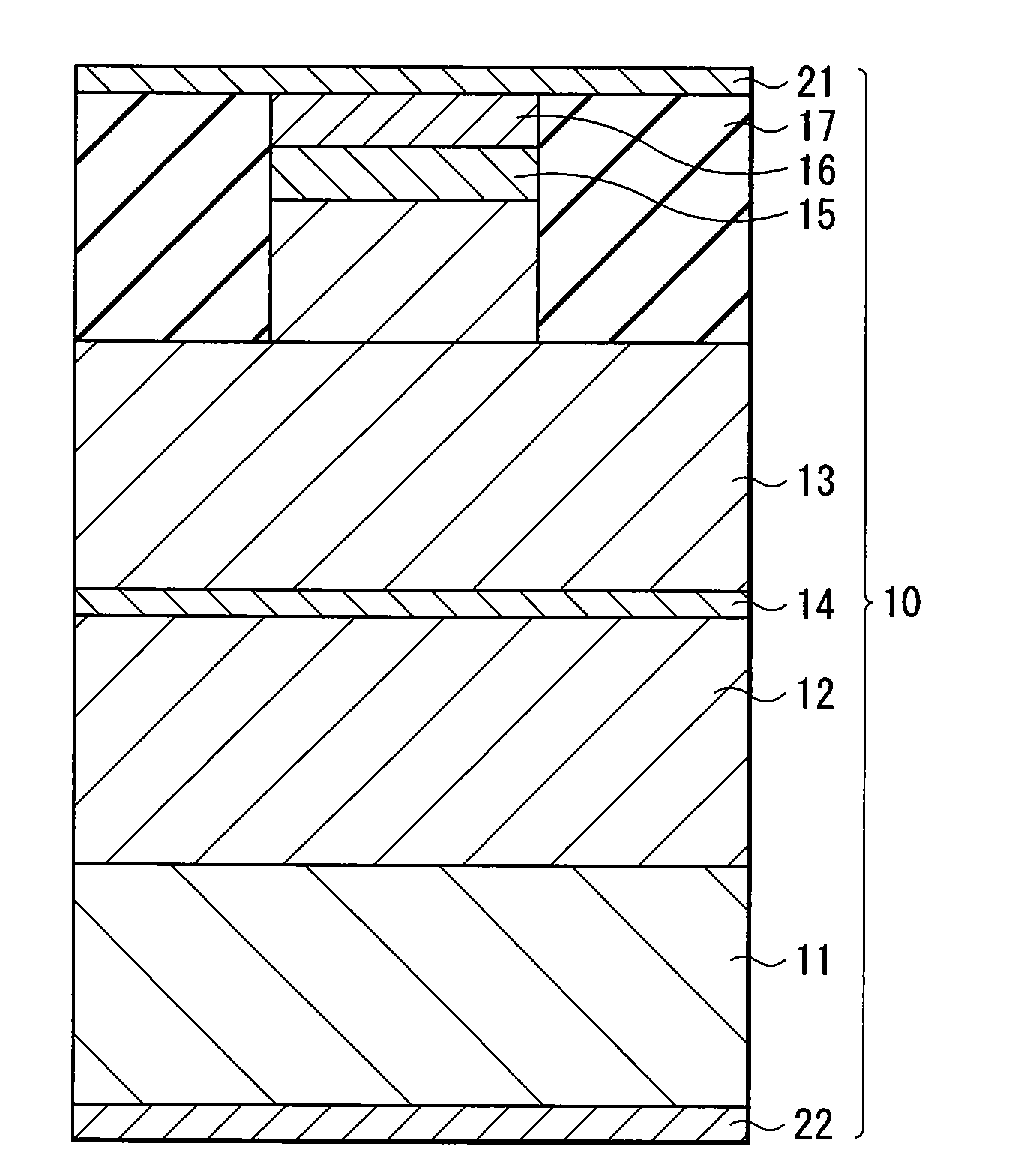
[0026]FIG. 1 shows the configuration of a main part of a laser diode according to an embodiment of the invention. A laser diode 10 is, for example, a green laser diode with a wavelength of 500 nm to 600 nm used for a laser pointer, and includes an active layer 14 between an n-type cladding layer 12 and a p-type cladding layer 13 which is made of a Group II-VI compound semiconductor. The n-type cladding layer 12, the active layer 14 and the p-type cladding layer 13 are laminated in order on a substrate 11 made of, for example, InP, and a superlattice layer 15 and a cap layer 16 are formed in order on the p-type cladding layer 13.

[0027]The n-type cladding layer 12 has, for example, a thickness in a laminate direction (hereinafter simply referred to as thickness) of 0.5 μm, and has a superlattice structure in which MgSe layers and Zn0.48Cd0.52Se mixed crystal layers are alternately lam...


PUM


Abstract

A semiconductor light-emitting device capable of increasing the carrier concentration of a p-type cladding layer and improving light-emitting efficiency is provided. A semiconductor light-emitting device is made of a Group II-VI compound semiconductor, and the semiconductor light-emitting device includes an active layer between an n-type cladding layer and a p-type cladding layer, in which the active layer has a Type II superlattice structure, and the junctions between the active layer and the n-type cladding layer and between the active layer and the p-type cladding layer each have a Type I structure, and the p-type cladding layer includes tellurium (Te) as a Group VI element.

Description

CROSS REFERENCES TO RELATED APPLICATIONS[0001]The present invention contains subject matter related to Japanese Patent Application JP 2007-097141 filed in the Japanese Patent Office on Apr. 3, 2007, the entire contents of which being incorporated herein by reference.BACKGROUND OF THE INVENTION[0002]1. Field of the Invention[0003]The present invention relates to a semiconductor light-emitting device such as a laser diode or a LED (Light Emitting Diode), and more specifically to a semiconductor light-emitting device suitable for emitting light in a green region with a wavelength of 500 nm to 600 nm.[0004]2. Description of the Related Art[0005]Laser diodes have been practically used in various fields as light-emitting devices with a small size and high reliability. In particular, a principal application of a laser diode emitting light in a visible to infrared region is optical recording such as optical disks, and as practically used laser diodes emitting light in a visible to infrared ...

Claims


Application Information

Patent Timeline
IPC IPC(8): H01S5/327
CPCB82Y20/00H01L33/06H01L33/28H01L33/285H01S5/2231H01S5/3216H01S5/3422H01S5/347
Inventor KISHINO, KATSUMINOMURA, ICHIROTASAI, KUNIHIKOTAMAMURA, KOSHINAKAJIMA, HIROSHINAKAMURA, HITOSHI
Owner HITACHI LTD
Why Eureka
Try Eureka