

Apparatus and method for detecting transparent substances
- Summary
- Abstract
- Description
- Claims
- Application Information
AI Technical Summary
Benefits of technology
Problems solved by technology
Method used
Image

Examples
first embodiment
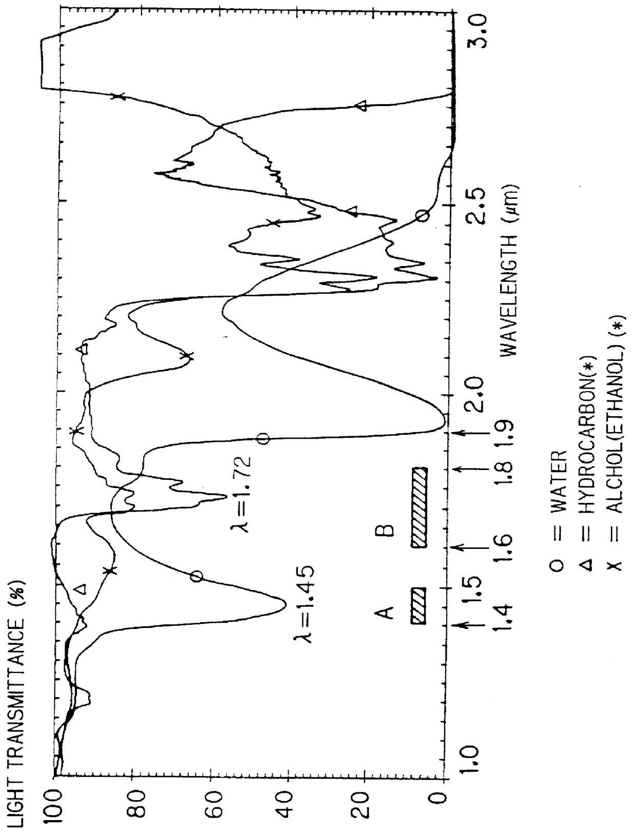
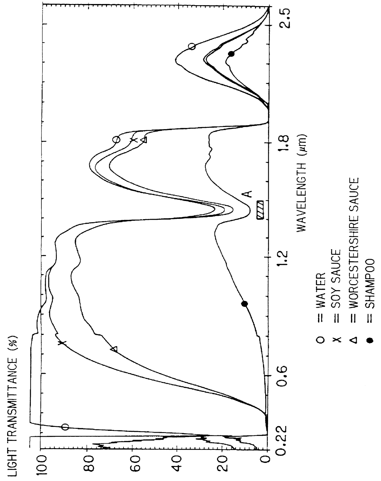
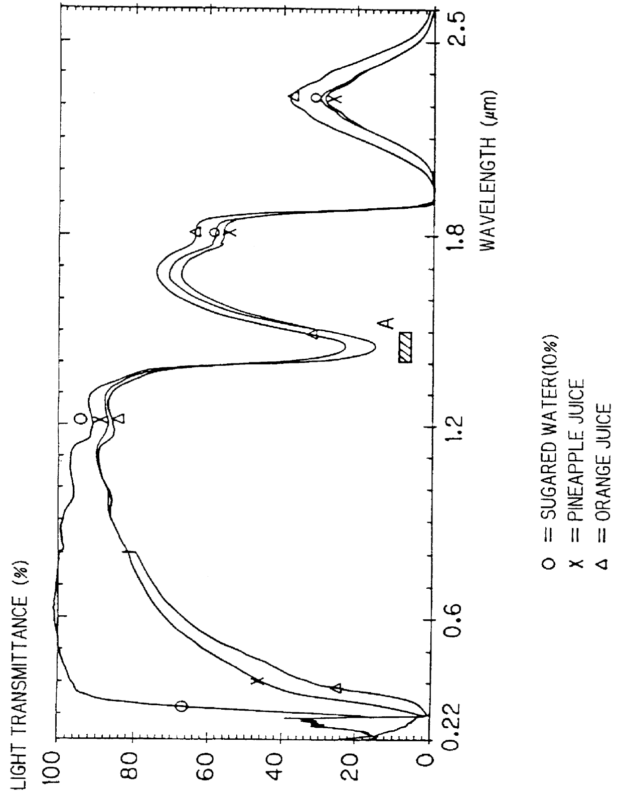
FIG. 10 is an appearance diagram of a reflection type photoelectric switch 1 which is a first embodiment of the present invention, and FIG. 11 is a block diagram showing its internal structure. This photoelectric switch 1 is used as (1) a detection photoelectric switch for a substance containing an OH group (concretely a liquid mainly composed of water), or (2) a detection photoelectric switch for a substance containing a CH.sub.2 group or a CH.sub.3 group (concretely an organic liquid containing these groups) in accordance with an emission wavelength of a semiconductor light-emitting device contained therein (which will be described later).
As shown in FIGS. 10 and 11, the photoelectric switch 1 contains an element group 10 in the interior of a rectangular parallelopiped casing 2. This element group 10 is roughly classified into a projecting system, a photoreceiving system and a switching system. Excitation power is generated in a light emission control circuit 11 and supplied to a ...
second embodiment
FIG. 12 is an appearance diagram of a transmission type photoelectric switch 100 which is a second embodiment of the present invention, and FIG. 13 is a block diagram showing its internal structure. Among these, FIG. 13 illustrates a mode in which the photoelectric switch 100 is used for level detection of a liquid mainly composed of water or an organic liquid.
As shown in FIG. 12, this photoelectric switch 100 consists of a combination of a projecting part 200 and a photoreceiving part 300, and these are set on positions opposed to each other and used as shown in FIG. 13. In a space therebetween, a detection object Q is stored in a container 50 formed by a material having small light absorption in an emission wavelength of a semiconductor light-emitting device 212, such as glass, for example.
The projecting part 200 comprises a light emission control circuit 211 and the semiconductor light-emitting device 212 of FIG. 13 in the interior of a rectangular parallelopiped casing 202 of FI...
third embodiment
FIG. 15 is an appearance diagram of a reflection type multi-wavelength photoelectric switch 401 which is an embodiment of the present invention, and FIG. 16 is a diagram showing the internal structure of the multi-wavelength photoelectric switch 401. The multi-wavelength photoelectric switch 401 is adapted to detect whether or not detection objects W (FIG. 19) contain water as a typical example of a substance having an OH group, without being influenced by surface states thereof with respect to two types of detection objects Wx and Wy whose surface states (colors, gloss and the like) are different from each other. The structure of the multi-wavelength photoelectric switch 401, an irradiation method of light, and a method of photoreceiving are now described.
The multi-wavelength photoelectric switch 401 is formed by a rectangular parallelopiped casing 402, a circuit group 410 in the interior of the casing 402, a fiber unit 403 which is an optical path means projecting light to the det...
PUM
 Abstract
Description
Claims
Application Information