
Dummy patterns for aluminum chemical polishing (CMP)
a technology of aluminum and chemical polishing, applied in the direction of grinding/polishing apparatus, grinding machines, manufacturing tools, etc., can solve the problems of metal erosion, metal dishing, and non-planar surface, so as to reduce the difference between high and low pattern factors on the chip, reduce erosion or dishing, and increase the uniformity of metal circuitry
- Summary
- Abstract
- Description
- Claims
- Application Information
AI Technical Summary
Benefits of technology
Problems solved by technology
Method used
Image

Examples
Embodiment Construction
)
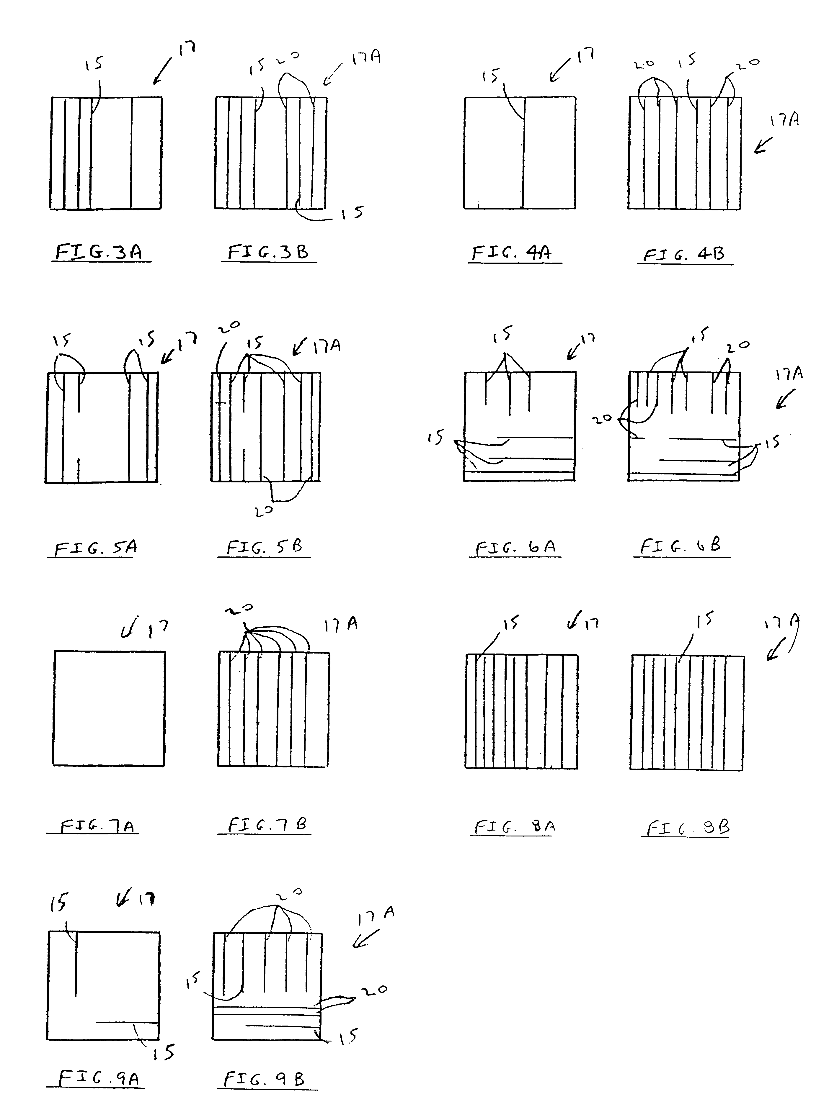
In describing the preferred embodiments of the present invention, reference will be made herein to FIGS. 1-11D of the drawings in which like numerals refer to like features of the invention. Features of the invention are not necessarily shown to scale in the drawings.
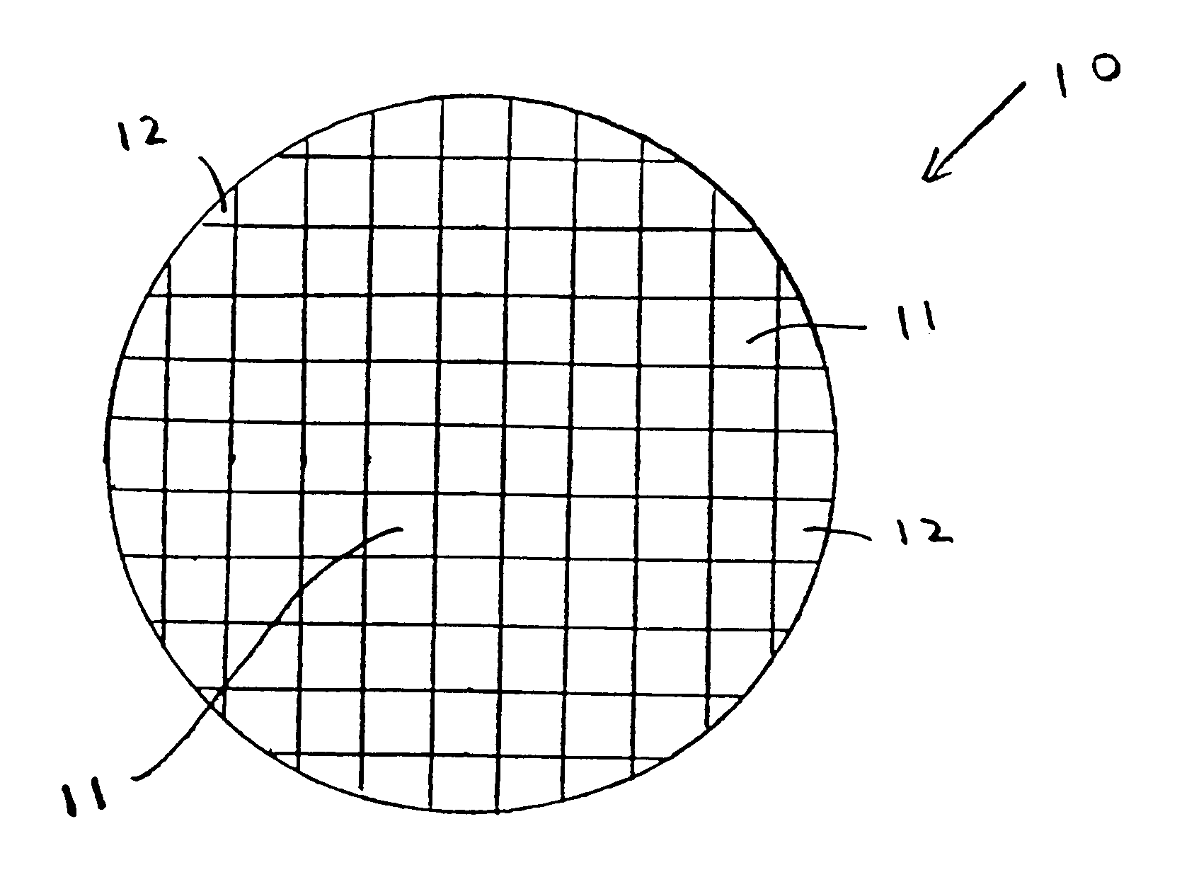
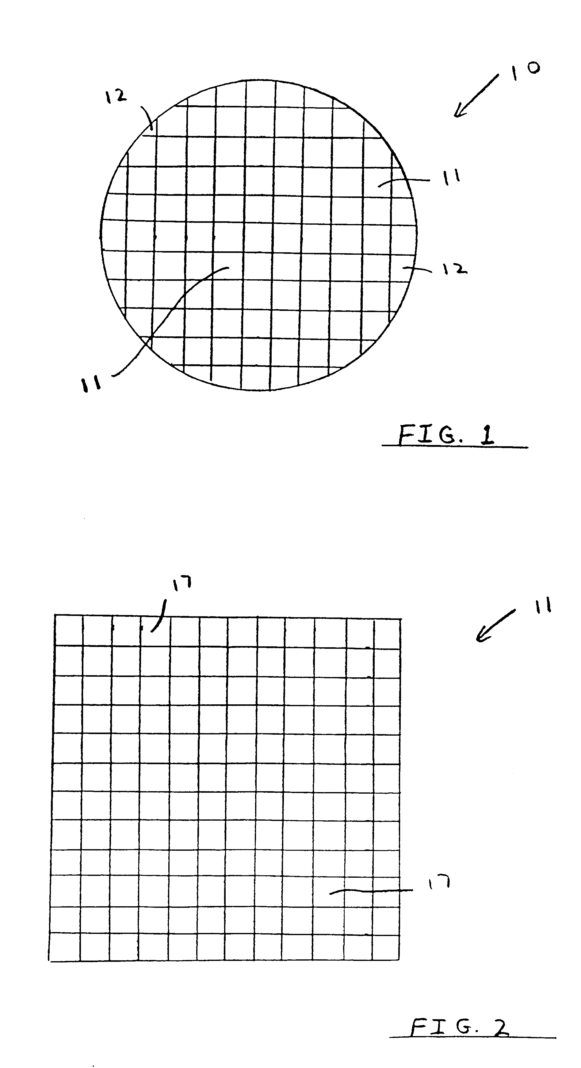
Referring to the drawings, FIG. 1 shows a conventional wafer 10 which is divided into a number of discrete chips 11. At the periphery of the wafer 10 are a number of areas designated 12 which represent parts of the wafer on which circuitry is not formed and which are discarded after the wafer is fabricated and the wafer cut to form integrated circuit devices.
FIG. 2 is an enlarged view of a chip 11 on wafer 10. The chip 11 is divided into a number of regions 17 and each region typically has circuitry thereon. The number of regions 17 in which the chip 11 may be divided is not critical, but, in general, the larger the number of regions, the more uniform (planar) the wafer will be after the CMP process. Typically up to ab...
PUM
| Property | Measurement | Unit |
|---|---|---|
| area | aaaaa | aaaaa |
| size | aaaaa | aaaaa |
| diameter | aaaaa | aaaaa |
Abstract
Description
Claims
Application Information