Dummy patterns for aluminum chemical polishing (CMP)

a technology of aluminum and pattern, applied in the field of system and method for polishing semiconductor wafers, can solve the problems of non-planar surface, particularly serious dishing effect, metal erosion, etc., and achieve the effect of less distortion or dishing, and less erosion or dishing

Inactive Publication Date: 2000-07-25
SAMSUNG ELECTRONICS CO LTD +1
View PDF17 Cites 117 Cited by
  • Summary
  • Abstract
  • Description
  • Claims
  • Application Information

AI Technical Summary

Benefits of technology

To overcome the dishing effect and other non-planarization, the invention decreases the differences in pattern factors for regions on the chip. For example, for HPF areas of up to 90% as compared to LPF areas of 0% or 20-30%, the difference in pattern factor may be as high as 90%. It is one aspect of the invention to decrease the difference in pattern factor across the chip surface by providing a uniform metal density (pattern factor) across the surface of the chip and, concomitantly, of the wafer.
In a further aspect of the invention, a predetermined low pattern factor design limit is set. For a lower limit of, for example, 20-50%, differences between the high and low pattern factors on the chip are minimized.
In a preferred aspect of the invention, a high pattern factor design limit and a low pattern factor design limit are both defined which will result in increased metal circuitry uniformity across the chip and wafer surface. For example, if the HPF limit is set at a maximum of 70% to 80% and a LPF limit at a minimum of 40% to 50%, the circuit density of the areas will differ by only 20% to 40% across the surface of the chip and wafer and result in a metal surface which has significantly less erosion or dishing after CMP processing.
In another aspect of the invention, the lower pattern factor design limit can be artificially generated for any given region on the chip or wafer surface by using a dummy circuit design. While it is preferred that an upper pattern factor limit also be used, this is not necessary and the use of a dummy circuit pattern layout will minimize the difference in circuit density over the chip and wafer surface and provide for a uniform metal surface after CMP.

Problems solved by technology

Unfortunately, problems such as dishing occur causing a non-planar surface.
The dishing effect is particularly serious since the polishing needs to be carried out until the metal is cleared on the entire wafer, i.e., wherein the metal is left exclusively in previously etched lines without any metal on the surface of the dielectric.
It has been found that a significant overpolish is typically needed which results in erosion of dielectric and dishing of metal as much as 100 nm below the level of the dielectric surface.
Additionally, an uneven topography is introduced on the wafer surface after CMP which will be repeated with slight attenuation after subsequent deposition of dielectric layers problems at later steps in the fabrication process.
Since the polishing needs to be carried out until the patterned metal is cleared on the entire wafer leaving metal exclusively in previously etched lines, HPF areas generally experience a significant overpolish resulting in erosion of the dielectric and dishing of metal up to 100 nm below the level of the dielectric surface.

Method used


Image

  • Dummy patterns for aluminum chemical polishing (CMP)
  • Dummy patterns for aluminum chemical polishing (CMP)
  • Dummy patterns for aluminum chemical polishing (CMP)

Examples


Embodiment Construction

)

In describing the preferred embodiments of the present invention, reference will be made herein to FIGS. 1-11D of the drawings in which like numerals refer to like features of the invention. Features of the invention are not necessarily shown to scale in the drawings.

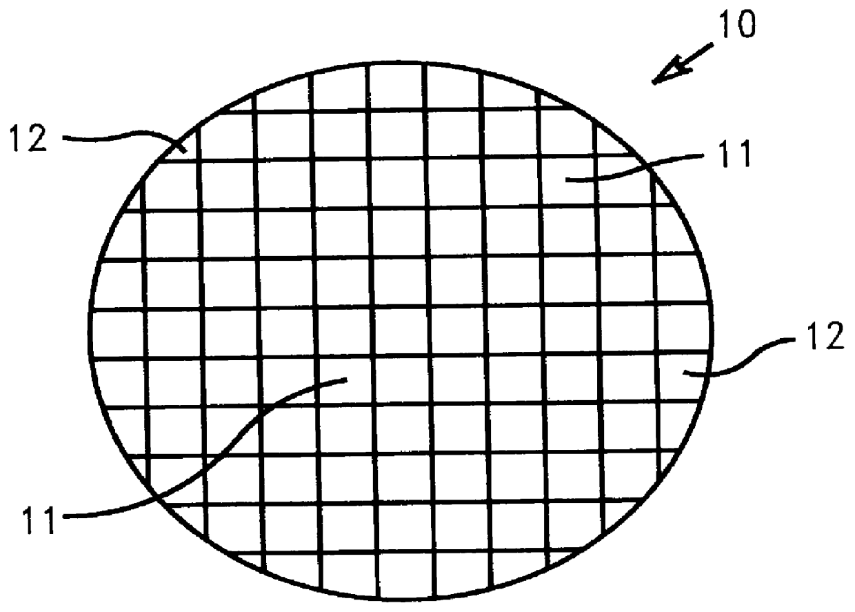
Referring to the drawings, FIG. 1 shows a conventional wafer 10 which is divided into a number of discrete chips 11. At the periphery of the wafer 10 are a number of areas designated 12 which represent parts of the wafer on which circuitry is not formed and which are discarded after the wafer is fabricated and the wafer cut to form integrated circuit devices.

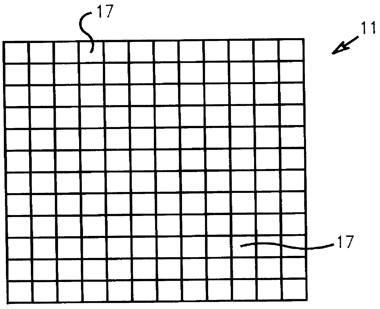
FIG. 2 is an enlarged view of a chip 11 on wafer 10. The chip 11 is divided into a number of regions 17 and each region typically has circuitry thereon. The number of regions 17 in which the chip 11 may be divided is not critical, but, in general, the larger the number of regions, the more uniform (planar) the wafer will be after the CMP process. Typically up to ab...


PUM


Abstract

A method and apparatus is provided for planarizing damascene metallic circuit patterns of a plurality of discrete integrated circuit chips on a metal coated silicon wafer wherein the circuitry on the chips on the wafer are either designed to be within a defined high metal density circuit range and low density metal circuit range and / or to provide dummy circuitry in the damascene process to provide a substantially uniform circuit density over the chip and the wafer surface. It is preferred that each chip on the surface of the wafer be divided into a plurality of regions and that each region be provided with dummy metallization, if necessary, to provide a relatively uniform circuit density in that region and consequently on the wafer surface. The invention also contemplates adding dummy circuitry to the periphery of the wafer in areas which are not formed into chips (chip fragments). The invention also provides semiconductor wafers made using the method and / or apparatus of the invention.

Description

1. Field of the InventionThe present invention relates to a system and method for polishing semiconductor wafers and, more particularly, to the polishing of damascene formed interconnects on the wafer using the chemical-mechanical polishing process in order to achieve a high degree of damascene planarity.2. Description of Related ArtIn the fabrication of integrated circuit devices, numerous integrated circuits are typically constructed simultaneously on a single semiconductor wafer. The wafer is then later divided by cutting the wafer into the individual integrated circuit devices.Typically, the integrated circuit device is made by a series of layering processes in which metallization, dielectrics, and other materials are applied to the surface of the wafer to form a layered interconnected structure. One important step in the fabrication process is to form interconnects in the insulator layers. The interconnects connect different layers of the integrated circuit device together and ...

Claims


Application Information

Patent Timeline
Patent Type & Authority Patents(United States)
IPC IPC(8): H01L21/02H01L21/321H01L21/304
CPCH01L21/3212Y10S438/926H01L21/027
Inventor JASO, MARK A.SCHNABEL, RAINER F.
Owner SAMSUNG ELECTRONICS CO LTD
Why Eureka
Try Eureka