Light emitting device and electronic apparatus using the same

a technology of light emitting devices and electronic devices, applied in the field of light emitting panels, can solve the problems of oversupplying voltage to the other pixels, and achieve the effects of suppressing the decrease of luminance, reducing luminance, and reducing luminan

Inactive Publication Date: 2007-01-02
SEMICON ENERGY LAB CO LTD
View PDF53 Cites 39 Cited by
  • Summary
  • Abstract
  • Description
  • Claims
  • Application Information

AI Technical Summary

Benefits of technology

[0012]In view of the foregoing, it is an object of the invention to provide a light emitting device capable of suppressing the luminance variations of the OLEDs associated with the deterioration of the organic light emitting material and achieving a consistent luminance.
[0015]Despite the varied degrees of deterioration of the light emitting elements of the pixels, the above arrangement eliminates the luminance variations for assuring the consistent luminance of the screen and also suppresses the decrease of luminance due to deterioration.
[0017]It is noted that a designer can arbitrarily define the reference pixel. As to those pixels more deteriorated than the reference pixel, the video signal may be so corrected as to increase the gradation levels of the pixels. As to those pixels less deteriorated than the reference pixel, the video signal may be so corrected as to lower the gradation levels of the pixels.

Problems solved by technology

At this time, an excessive voltage is supplied to the other pixels that share the common voltage source with the most deteriorated pixel.

Method used


Image

  • Light emitting device and electronic apparatus using the same
  • Light emitting device and electronic apparatus using the same
  • Light emitting device and electronic apparatus using the same

Examples


example 1

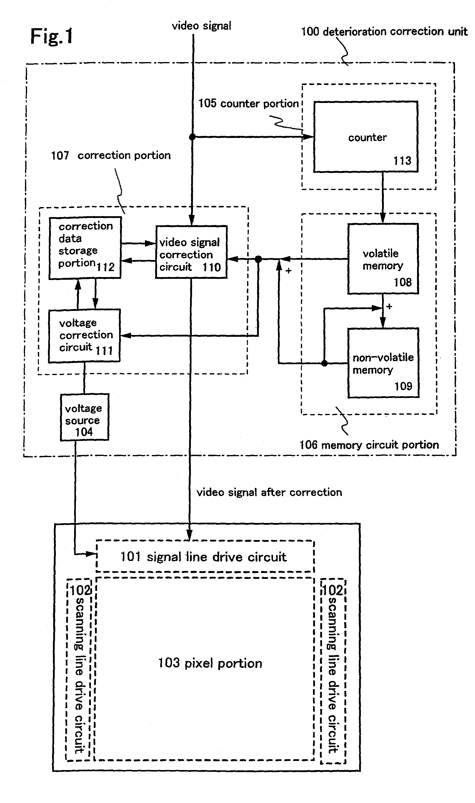
[0067]In this example, description is made on a method for correcting the video signal which is adopted by the correction portion of the light emitting device according to the invention.

[0068]In one approach to complement the decreased luminance of the deteriorated light emitting element on the basis of a signal, a given correction value is added to an input video signal to convert the input signal to a signal practically representing a gradation level increased by several steps thereby achieving a luminance equivalent to that prior to the deterioration. The simplest way to implement this approach in circuit design is to provide a circuit in advance which is capable of processing data on an extra gradation level.

[0069]Specifically, in the case of a light emitting element adapted for 6-bit digital gradations (64 gradation levels) and including the deterioration correction function of the invention, for example, the device is so designed and manufactured as to have an additional capab...

example 2

[0070]In this example, description is made on a method for correcting the video signal in a different way from that of Example 1.

[0071]FIG. 5A is an enlarged view showing the pixel portion 103 of FIG. 1. Here, three pixels 201 to 203 are discussed. It is assumed that the pixel 201 suffers the least deterioration, the pixel 202 suffering a greater deterioration than the pixel 201, the pixel 203 suffering the greatest deterioration.

[0072]The greater the deterioration of the pixel, the greater the decrease of luminance of the pixel. Without the correction of luminance, the pixels, which are displaying a certain half tone, will encounter luminance variations as shown in FIG. 5B. That is, the pixel 202 presents a lower luminance than the pixel 201 whereas the pixel 203 presents a much lower luminance than the pixel 201.

[0073]Next, actual correction operations are described. Measurement is previously taken to obtain a relation between the accumulative data on the light emission periods or...

example 3

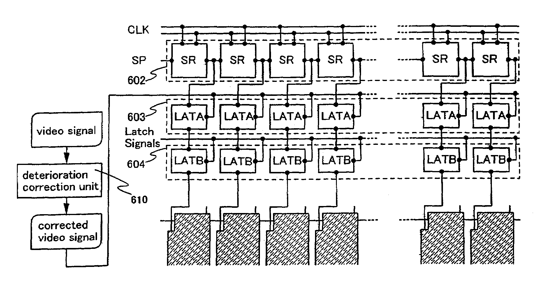
[0086]In Example 3, the following description refers to the configurations of a signal line drive circuit and a scanning line drive circuit provided for the light emitting device of the present invention.

[0087]The block figure of a drive circuit in a light emitting device with respect to this example is shown in FIGS. 6A and 6B. FIG. 6A shows the signal line drive circuit 601, which has a shift register 602, a latch (A) 603, and a latch (B) 604.

[0088]FIG. 6B shows a further detailed configuration of the signal line drive circuit shown in FIG. 6A.

[0089]A clock signal CLK and a start pulse SP are input to the shift register 602 in the signal line drive circuit 601. The shift register 602 generates timing signals in order based upon the clock signal CLK and the start pulse SP, and supplies the timing signals one after another to the subsequent stage circuit through the buffer (not illustrated) and the like.

[0090]Note that, the timing signals output from the shift register circuit 602 m...


PUM


Abstract

Providing a light emitting device capable of suppressing the variations of luminance of OLEDs associated with the deterioration of an organic light emitting material, and achieving a consistent luminance. An input video signal is constantly or periodically sampled to sense a light emission period or displayed gradation level of each of light emitting elements of pixels and then, a pixel suffering the greatest deterioration and decreased luminance is predicted from the accumulations of the sensed values. A voltage supply to the target pixel is corrected for achieving a desired luminance. The other pixels than the target pixel are supplied with an excessive voltage and hence, the individual gradation levels of the pixels are lowered by correcting the video signal for driving the pixel with the deteriorated light emitting element on as-needed basis, the correction of the video signal made by comparing the accumulation of the sensed values of each of the other pixels with a previously stored data on a time-varying luminance characteristic of the light emitting element.

Description

BACKGROUND OF THE INVENTION[0001]1. Field of the Invention[0002]The present invention relates to a light emitting panel in which a light emitting element formed on a substrate is enclosed between the substrate and a cover member. Also, the present invention relates to a light emitting module in which an IC or the like is mounted on the light emitting panel. Note that, in this specification, the light emitting panel and the light emitting module are generically called light emitting devices. The present invention further relates to electronic apparatuses utilizing the light emitting devices.[0003]2. Description of the Related Art[0004]A light emitting element emits light by itself, and thus, has high visibility. The light emitting element does not need a backlight necessary for a liquid crystal display device (LCD), which is suitable for a reduction of a light emitting device in thickness. Also, the light emitting element has no limitation on a viewing angle. Therefore, recently, the...

Claims


Application Information

Patent Timeline
Patent Type & Authority Patents(United States)
IPC IPC(8): G09G5/10G09G3/30G09G3/20G09G3/32
CPCG09G3/3233G09G3/3291G09G3/2022G09G2300/0842G09G2310/0251G09G2360/18G09G2320/0233G09G2320/029G09G2320/043G09G2320/048G09G2310/027G09G3/30
Inventor YAMAZAKI, SHUNPEIKOYAMA, JUN
Owner SEMICON ENERGY LAB CO LTD
Why Eureka
Try Eureka