
Semiconductor integrated apparatus and black level correction method for image sensor

a technology of image sensor and integrated apparatus, which is applied in the direction of color television, television system, color signal processing circuit, etc., can solve the problem of level reference value taking time, and achieve the effect of suppressing the variation in image brightness and shortening the tim

Inactive Publication Date: 2011-04-05
SOCIONEXT INC
View PDF6 Cites 5 Cited by
  • Summary
  • Abstract
  • Description
  • Claims
  • Application Information

AI Technical Summary

Benefits of technology

The present invention relates to a semiconductor integrated apparatus that can suppress a variation in brightness of an image and make a reference value of a black level converge at an appropriate value in a short time. The apparatus includes a variable gain amplifier for amplifying the pixels value detected by an image sensor, a black level correction circuit for making a new black level reference value if the amount of change in gains of the variable gain amplifier exceeds a predetermined value for a predetermined period of time. The apparatus can automatically control the gain of the variable gain amplifier based on the valid pixel and the previous black level reference value. The technical effect of the invention is to suppress a variation in brightness of the image and make the reference value of the black level converge at an appropriate value in a short time.

Problems solved by technology

This brings forth a problem of the black level reference value taking time for converging on a appropriate value.

Method used


Image

  • Semiconductor integrated apparatus and black level correction method for image sensor
  • Semiconductor integrated apparatus and black level correction method for image sensor
  • Semiconductor integrated apparatus and black level correction method for image sensor

Examples


first embodiment

[0061]FIG. 7 is a circuit block diagram of a semiconductor integrated apparatus (i.e., a semiconductor integrated circuit) 21 including a black level correction circuit according to a

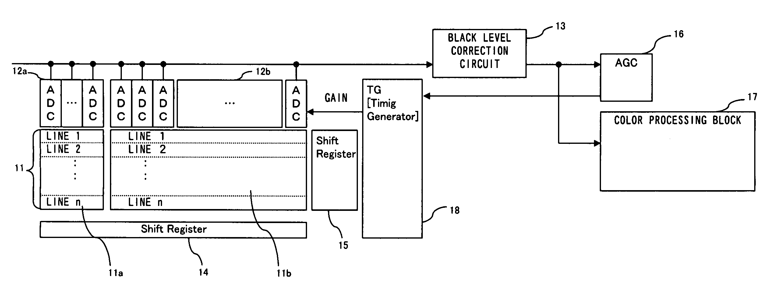
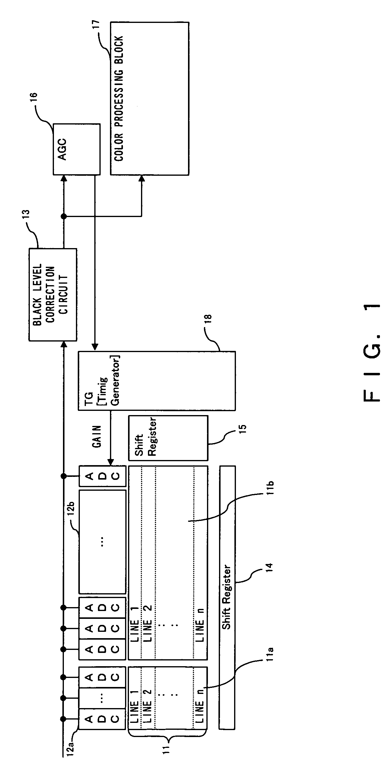
[0062]A black level pixel value output from a shaded part from light 11a (simply a “shaded part 11a” hereinafter) of an image sensor 11 (refer to FIG. 1) is amplified by a variable gain amplifier 22 and converted to digital image data by an A / D converter 23. Meanwhile, a pixel value of a valid pixel output from an imaging part 11b of the image sensor 11 is amplified by a variable gain amplifier 24 and converted to digital valid image data by an A / D converter 25.

[0063]A register group 29 comprises a register 30 for storing the number of judgment frames (corresponding to a predetermined period), a register 31 for storing a multiplier value N for multiplying a black level average value of the current frame, a register 32 for storing a multiplier value M for multiplying a weighted average of the past frames...

second embodiment

[0123]The second embodiment is configured to judge whether or not a frame of an amount of change in gains of a black level value being equal to or greater than a predetermined value (i.e., a threshold value) continues for a predefined number of frames, and change black reference data to the black level value of the current frame if the aforementioned frame continues for the predefined number of frames or more.

[0124]Referring to FIG. 14, an average calculation circuit 51 (refer to FIG. 9) calculates the average value of black level data (simply called a “black level a” hereinafter) of the current frame which is detected by a shaded part 11a of an image sensor 11 and A / D converted.

[0125]The average value of the black level data calculated by the average calculation circuit 51 is output to a latch circuit 103 and a weighted average calculation circuit 52 (refer to FIG. 9).

[0126]The latch circuit 103 latches black level data output from the average calculation circuit 51 at a timing syn...


PUM


Abstract

The challenge of the present invention is to suppress a variation in brightness of an image and make a reference value of a black level converge at an appropriate value in a short time. A condition judgment circuit judges whether or not a frame of an amount of change in gains of a variable gain amplifier being equal to or greater than a threshold continues for a predefined frames or more. If a frame of an amount of change in the gains being equal to or greater than the threshold continues for the predefined frames, a black level value of the current frame is set for new black level reference. If not continues for the predetermined number, the previous black level reference value is retained in lieu of correcting the black level.

Description

CROSS REFERENCE TO RELATED APPLICATIONS[0001]This application is based upon and claims the benefit of priority from the prior Japanese Patent Application No. 2005-288744 filed on Sep. 30, 2005, the entire contents of which are incorporated herein by reference.BACKGROUND OF THE INVENTION[0002]1. Field of the Invention[0003]The present invention relates to a semiconductor integrated apparatus having a black level correction circuit for an image sensor and a black level correction method therefor.[0004]2. Description of the Related Art[0005]A semiconductor image sensor such as a CMOS (complementary metal-oxide semiconductor) sensor changes an output level thereof due to a temperature change, et cetera, resulting in an imaged image becoming lighter or darker due to a temperature change even if the same imaging object is imaged. In order to eliminate such a problem, a fluctuation of an output of an image sensor due to a temperature change, et cetera, is suppressed by shading a part there...

Claims


Application Information

Patent Timeline
Patent Type & Authority Patents(United States)
IPC IPC(8): H04N5/217H04N25/00
CPCH04N5/361H04N25/63H04N23/82
Inventor KOKUBO, ASAODAIKU, HIROSHIFUNAKOSHI, JUNHIGUCHI, TSUYOSHI
Owner SOCIONEXT INC
Learn More