Display device

a display device and driving configuration technology, applied in the field of display devices, can solve the problems of preventing the adoption of the mechanism described in the patent document 2, affecting the achievement of the higher definition of the display device, and it is difficult to apply the driving configuration of the 5tr driving configuration to the display device used in a small electronic device such as a portable device (mobile device), and achieve the effect of cost reduction

Inactive Publication Date: 2014-02-27
JOLED INC
View PDF6 Cites 5 Cited by
  • Summary
  • Abstract
  • Description
  • Claims
  • Application Information

AI Technical Summary

Benefits of technology

[0023]The present invention has been made in view of the above situation. First, it is desirable to provide a mechanism that directing attention to a vertical scanning system, allows a vertical scanning line and a vertical scanning signal to be shared between a plurality of pixels (that is, a plurality of rows) without increasing the number of control lines or control signals.
[0024]Further, it is desirable to provide a mechanism that makes it possible to achieve higher definition of a display device by simplifying a pixel circuit. In addition, it is desirable to provide a mechanism that can suppress luminance change due to variations in characteristics of a driving transistor and an electrooptic element in simplifying a pixel circuit.
[0033]Thus, cost reduction can be achieved by sharing a writing scanning line of vertical scanning lines and a writing driving pulse supplied to pixel circuits via the writing scanning line between pixel circuits of a plurality of rows without increasing the number of control lines or control signals.

Problems solved by technology

However, the mechanism described in Patent Document 2 may not be adopted into a mechanism that makes mobility correction by performing signal writing while passing current when driving a current-driven type electrooptic element.
Many constituent elements of the pixel circuit hinder achievement of higher definition of the display device.
As a result, it is difficult to apply the 5TR driving configuration to a display device used in a small electronic device such as a portable device (mobile device) or the like.

Method used


Image

  • Display device
  • Display device
  • Display device

Examples


first example

Pixel Circuit of Comparative Example

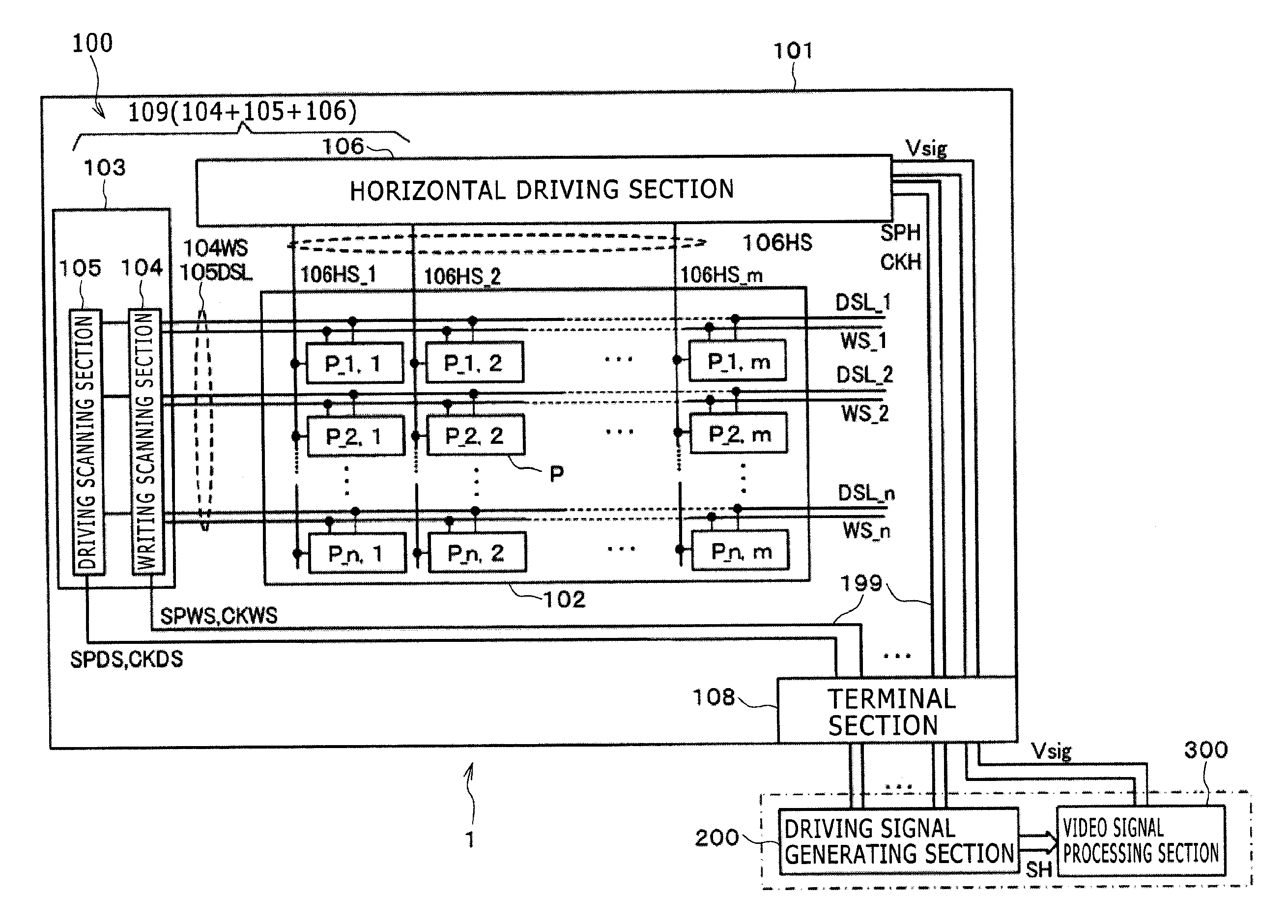
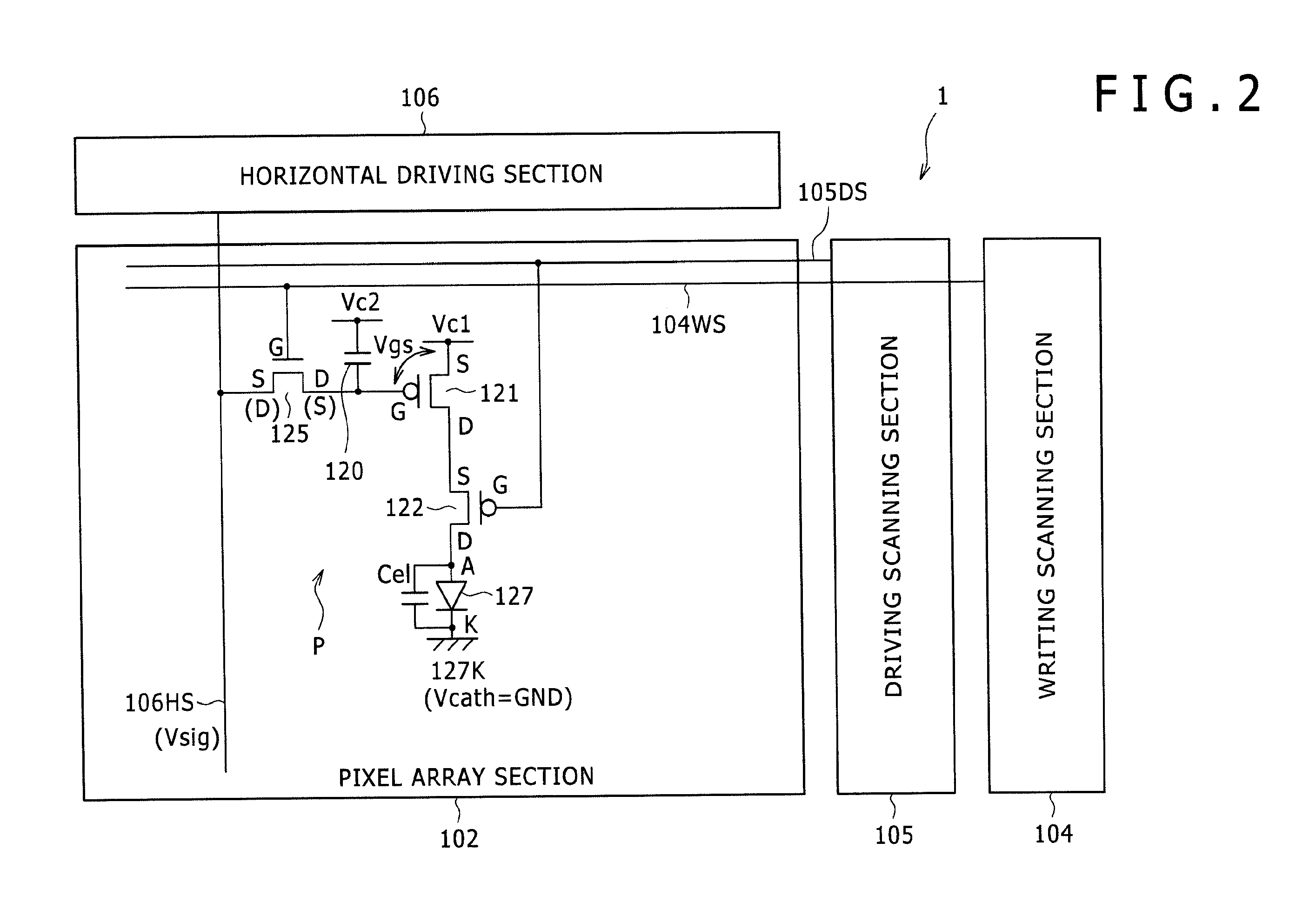
[0078]As shown in FIG. 2, the pixel circuit P according to the first comparative example is basically defined in that a driving transistor is formed by a p-type thin film field-effect transistor (TFT). In addition, the pixel circuit P according to the first comparative example employs a 3Tr driving configuration using two transistors for scanning in addition to the driving transistor.

[0079]Specifically, the pixel circuit P according to the first comparative example includes the p-type driving transistor 121, a p-type light emission controlling transistor 122 supplied with an active-L driving pulse, an n-type transistor 125 supplied with an active-H driving pulse, an organic EL element 127 as an example of an electrooptic element (light emitting element) that emits light by being fed with a current, and a storage capacitor (referred to also as a pixel capacitance) 120. Incidentally, a simplest circuit can employ a 2Tr driving configuration from whi...

second example

Pixel Circuit of Comparative Example

[0089]A pixel circuit P according to the second comparative example shown in FIG. 3 will next be described as a comparative example in describing characteristics of the pixel circuit P according to the present embodiment. The pixel circuit P according to the second comparative example (as with the present embodiment to be described later) is basically defined in that a driving transistor is formed by an n-type thin film field-effect transistor. When each transistor can be formed as an n-type rather than a p-type, an existing amorphous silicon (a-Si) process can be used in transistor production. Thereby, the transistor substrate can be reduced in cost. The development of pixel circuits P of such a constitution is anticipated.

[0090]The pixel circuit P according to the second comparative example is basically the same as the present embodiment to be described later in that a driving transistor is formed by an n-type thin film field-effect transistor. ...

third example

Pixel Circuit of Comparative Example

[0106]The pixel circuit P according to the third comparative example shown in FIG. 6, on which circuit the pixel circuit P according to the present embodiment is based, employs a driving system that incorporates a circuit (bootstrap circuit) for preventing variation in driving current due to a secular change of the organic EL element 127 in the pixel circuit P according to the second comparative example shown in FIG. 3, and which driving system prevents variation in driving current due to variation in the characteristics of the driving transistor 121 (variations in threshold voltage and variations in mobility).

[0107]As with the pixel circuit P according to the second comparative example, the pixel circuit P according to the third comparative example uses an n-type driving transistor 121. In addition, the pixel circuit P according to the third comparative example is defined in that the pixel circuit P according to the third comparative example has ...


PUM


Abstract

Disclosed herein is a display device that allows a vertical scanning line to be shared between a plurality of rows without increasing the number of control lines or control signals, the display device including pixel circuits; vertical scanning lines; and horizontal scanning lines.

Description

CROSS REFERENCES TO RELATED APPLICATIONS[0001]The present application is a Continuation application of Ser. No. 12 / 475,227, which was filed on May 29, 2009 and claims priority based on Japanese Priority Patent Application JP 2008-165203 filed in the Japan Patent Office on Jun. 25, 2008, the entire content of which is hereby incorporated by reference.BACKGROUND OF THE INVENTION[0002]1. Field of the Invention[0003]The present invention relates to a display device having a pixel circuit (referred to also as a pixel) provided with an electrooptic element (referred to also as a display element or a light emitting element), and particularly to a display device having a current-driven type electrooptic element changing in luminance according to the magnitude of a driving signal as a display element, and having an active element in each pixel circuit, display driving being performed in a pixel unit by the active element.[0004]2. Description of the Related Art[0005]There are display devices ...

Claims


Application Information

Patent Timeline
Patent Type & Authority Applications(United States)
IPC IPC(8): G09G3/32G09G3/36
CPCG09G3/3659G09G3/3258G09G3/3233G09G3/3266G09G2300/0426G09G2300/0819G09G2310/0262
Inventor YAMAMOTO, TETSUROUCHINO, KATSUHIDE
Owner JOLED INC
Why Eureka
Try Eureka