Method for driving display device

Inactive Publication Date: 2010-07-22
SEMICON ENERGY LAB CO LTD
View PDF27 Cites 52 Cited by
  • Summary
  • Abstract
  • Description
  • Claims
  • Application Information

AI Technical Summary

Benefits of technology

[0060]According to one embodiment of the present invention, the time during which a transistor is on can be reduced; degradation of characteristics of a transistor can be suppressed; the channel width of a transistor can be reduced; the layout area can be reduced; the frame of a display device can be reduced; higher definition of a display

Problems solved by technology

As such degradation of the transistor progresses, it becomes difficult to operate a driver circuit and incapable of displaying images

Method used


Image

  • Method for driving display device
  • Method for driving display device
  • Method for driving display device

Examples


embodiment 1

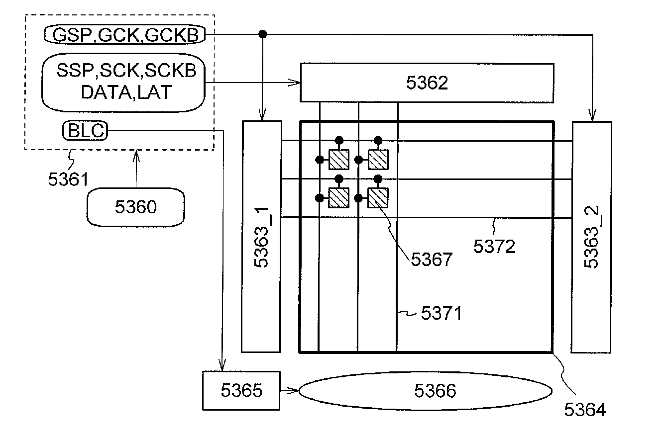
[0112]In this embodiment, an example of a semiconductor device will be described. The semiconductor device in this embodiment can be used for, for example, a shift register, a gate driver, a source driver, or a display device. Note that the semiconductor device in this embodiment can also be referred to as a driver circuit.

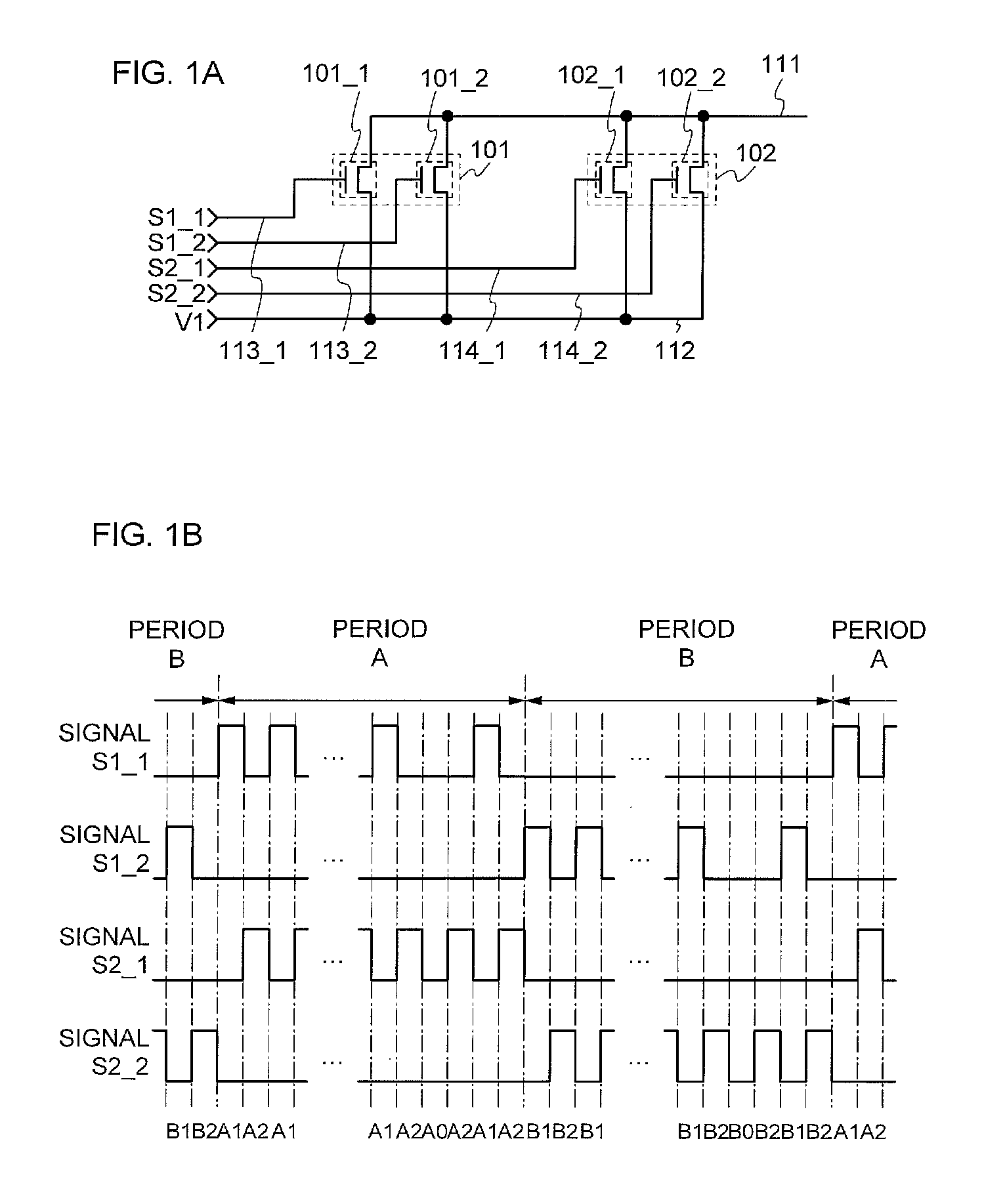
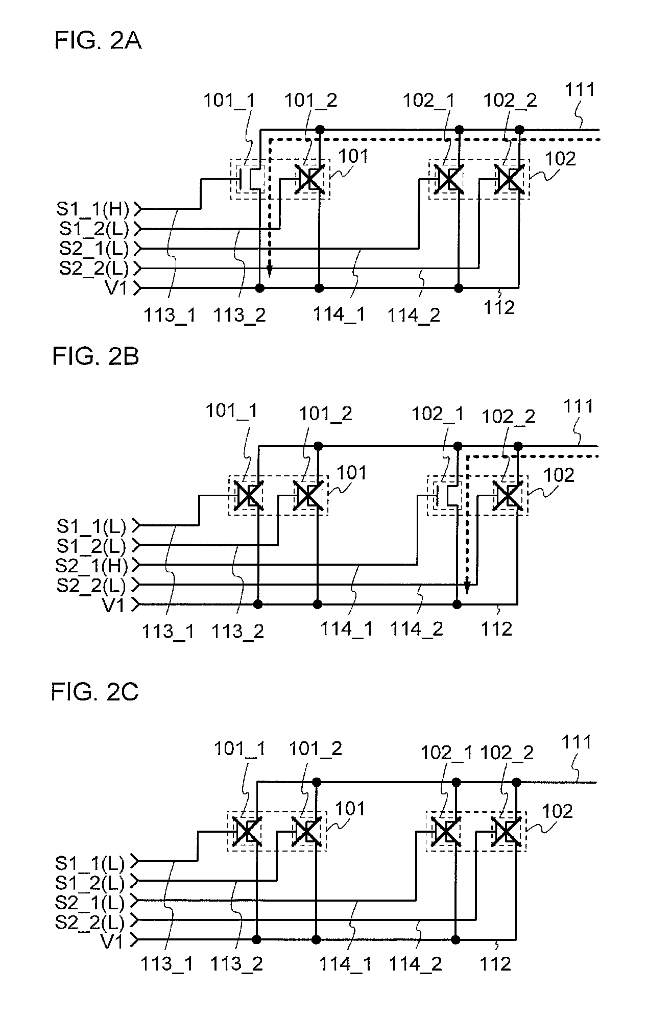
[0113]First, a basic circuit which can be used for the semiconductor device in this embodiment is described with reference to FIG. 41A. The circuit in FIG. 41A includes a plurality of circuits: a circuit 101 and a circuit 102. The circuit 101 includes a plurality of switches: a switch 11_1 and a switch 112. The circuit 102 includes a plurality of switches: a switch 12_1 and a switch 12_2. The switches 11_1, 11_2, 12_1, and 122 are connected between a wiring 111 and a wiring 112. Note that the circuit in FIG. 41A can also be referred to as a semiconductor device or a driver circuit.

[0114]The switches 11_1, 11_2, 12_1, and 12_2 have a function of controlling a condu...

embodiment 2

[0198]In this embodiment, an example of a semiconductor device will be described. The semiconductor device in this embodiment can include the semiconductor device in Embodiment 1. The semiconductor device in this embodiment can be used for, for example, a flip flop, a shift register, a gate driver, a source driver, or a display device. Note that the semiconductor device in this embodiment can also be referred to as a flip flop or a driver circuit.

[0199]First, an example of the semiconductor device in this embodiment is described with reference to FIG. 7A. The semiconductor device in FIG. 7A includes the circuit 101, the circuit 102, and a transistor 201. The circuit 101 includes a plurality of transistors: the transistor 101_1 and the transistor 1012. The circuit 102 includes a plurality of transistors: the transistor 102_1 and the transistor 102_2.

[0200]Note that the transistor 201 preferably has the same polarity as the transistors 101_1, 101_2, 102_1, and 102_2, and is often an n...

embodiment 3

[0254]In this embodiment, an example of the circuit 300 described in Embodiment 2 will be described. Note that the circuit 300 can be referred to as a semiconductor device, a driver circuit, or a gate driver. The contents described in Embodiments 1 and 2 are not repeated. Further, the contents described in Embodiments 1 and 2 can be freely combined with a content described in this embodiment.

[0255]First, an example of the circuit 300 is described with reference to FIG. 21A. The circuit 300 includes a transistor 301, a transistor 302, a transistor 303, a transistor 304_1, a transistor 304_2, a transistor 305_1, and a transistor 305_2. Note that this embodiment is not limited thereto, and the circuit 300 can include a variety of other components. Alternatively, any of the transistors in the circuit 300 can be omitted.

[0256]Note that the transistors 301, 302, 303, 304_1, 304_2, 305_1, and 305_2 preferably have the same polarity as the transistor 201, and are n-channel transistors. Note...


PUM


Abstract

To suppress degradation of a transistor. A method for driving a liquid crystal display device has a first period and a second period. In the first period, a first transistor and a second transistor are alternately turned on and off repeatedly, and a third transistor and a fourth transistor are turned off. In the second period, the first transistor and the second transistor are turned off, and the third transistor and the fourth transistor are alternately turned on and off repeatedly. Accordingly, the time during which the transistor is on can be reduced, so that degradation of characteristics of the transistor can be suppressed.

Description

BACKGROUND OF THE INVENTION[0001]1. Field of the Invention[0002]The present invention relates to a semiconductor device, a display device, a liquid crystal display device, a method for driving these devices, and a method for manufacturing these devices. The present invention particularly relates to a semiconductor device, a display device, and a liquid crystal display device which include a driver circuit formed over the same substrate as a pixel portion, and a method for driving these devices. Further, the present invention relates to an electronic device including the semiconductor device, the display device, or the liquid crystal display device.[0003]2. Description of the Related Art[0004]In recent years, with the increase of large display devices such as liquid crystal televisions, display devices have been actively developed. In particular, a technique for forming a driver circuit such as a gate driver over the same substrate as a pixel portion by using transistors including a ...

Claims


Application Information

Patent Timeline
IPC IPC(8): G06F3/038
CPCG09G3/3614G09G3/3677G09G3/3688G09G2310/0286G09G3/14G11C19/28G02F1/133G06F3/038G09G3/20G09G2320/043G09G3/3648G02F1/1362G09G2330/021G09G3/3291G09G3/3674G09G3/36G09G2300/0426H01L27/124
Inventor KIMURA, HAJIMEUMEZAKI, ATSUSHI
Owner SEMICON ENERGY LAB CO LTD
Why Eureka
Try Eureka