Organic electroluminescent display device, electronic apparatus including the same, and method for producing organic electroluminescent display device

a technology of electroluminescent display device and electronic apparatus, which is applied in the direction of solid-state devices, semiconductor devices, thermoelectric devices, etc., can solve the problems of forming a pixel, reducing the aperture ratio, and not increasing the power consumption of organic el displays, etc., to achieve wide color reproduction range, high definition, and low cost

Active Publication Date: 2014-10-23
SHARP KK
View PDF3 Cites 63 Cited by
  • Summary
  • Abstract
  • Description
  • Claims
  • Application Information

AI Technical Summary

Benefits of technology

[0033]According to the present invention, it is possible to provide an organic EL display device which is capable of achieving full-color display and higher definition at low cost and which has a wide color reproduction range and excellent viewing angle characteristics, and an electronic apparatus including the organic EL display device.

Problems solved by technology

Unlike liquid crystal displays, the power consumption of organic EL displays is not increased by the fact that a trend toward higher definition causes lower aperture ratios.
The conventional method for forming a pixel suffers from disadvantages, including mask processing accuracy, mask alignment accuracy, an increase in mask size, mask deformation, and color mixture due to thermal deformation.
However, white light is split into red-, green-, and blue-emitting components with a color filter, thus disadvantageously increasing the power consumption.

Method used


Image

  • Organic electroluminescent display device, electronic apparatus including the same, and method for producing organic electroluminescent display device
  • Organic electroluminescent display device, electronic apparatus including the same, and method for producing organic electroluminescent display device
  • Organic electroluminescent display device, electronic apparatus including the same, and method for producing organic electroluminescent display device

Examples


first embodiment

(1) First Embodiment

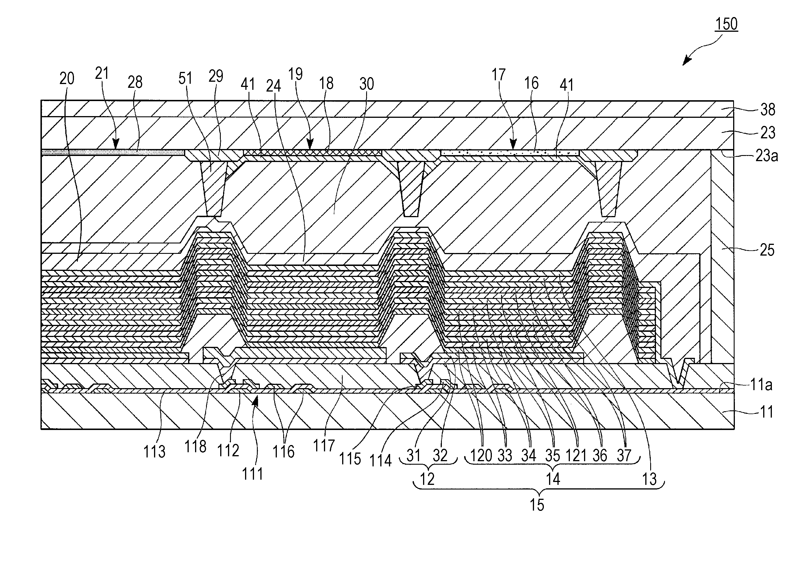
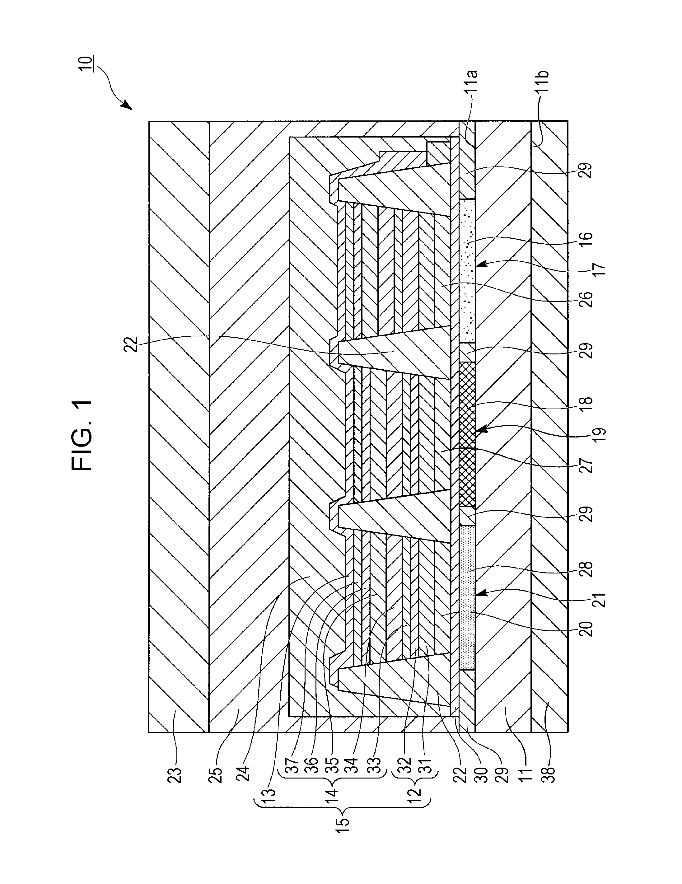
[0057]FIG. 1 is a schematic cross-sectional view of an organic electroluminescent display device (hereinafter, referred to as an “organic EL display device”) according to a first embodiment.

[0058]An organic EL display device 10 includes a first substrate 11; an organic electroluminescent section (hereinafter, referred to as an “organic EL section”) 15 disposed on a first surface 11a of the first substrate 11, the organic EL section 15 including an organic layer 14 held between a first electrode 12 and a second electrode 13; a blue pixel portion 17 including a blue color filter 16; a green pixel portion 19 including a green color filter 18; a red pixel portion 21 including a wavelength conversion layer 20 containing a wavelength conversion material; an edge cover (partition) 22 on the first surface 11a of the first substrate 11, the edge cover 22 being configured to surround side faces of portions of the organic EL section 15 to define pixels; and a second substra...

second embodiment

(2) Second Embodiment

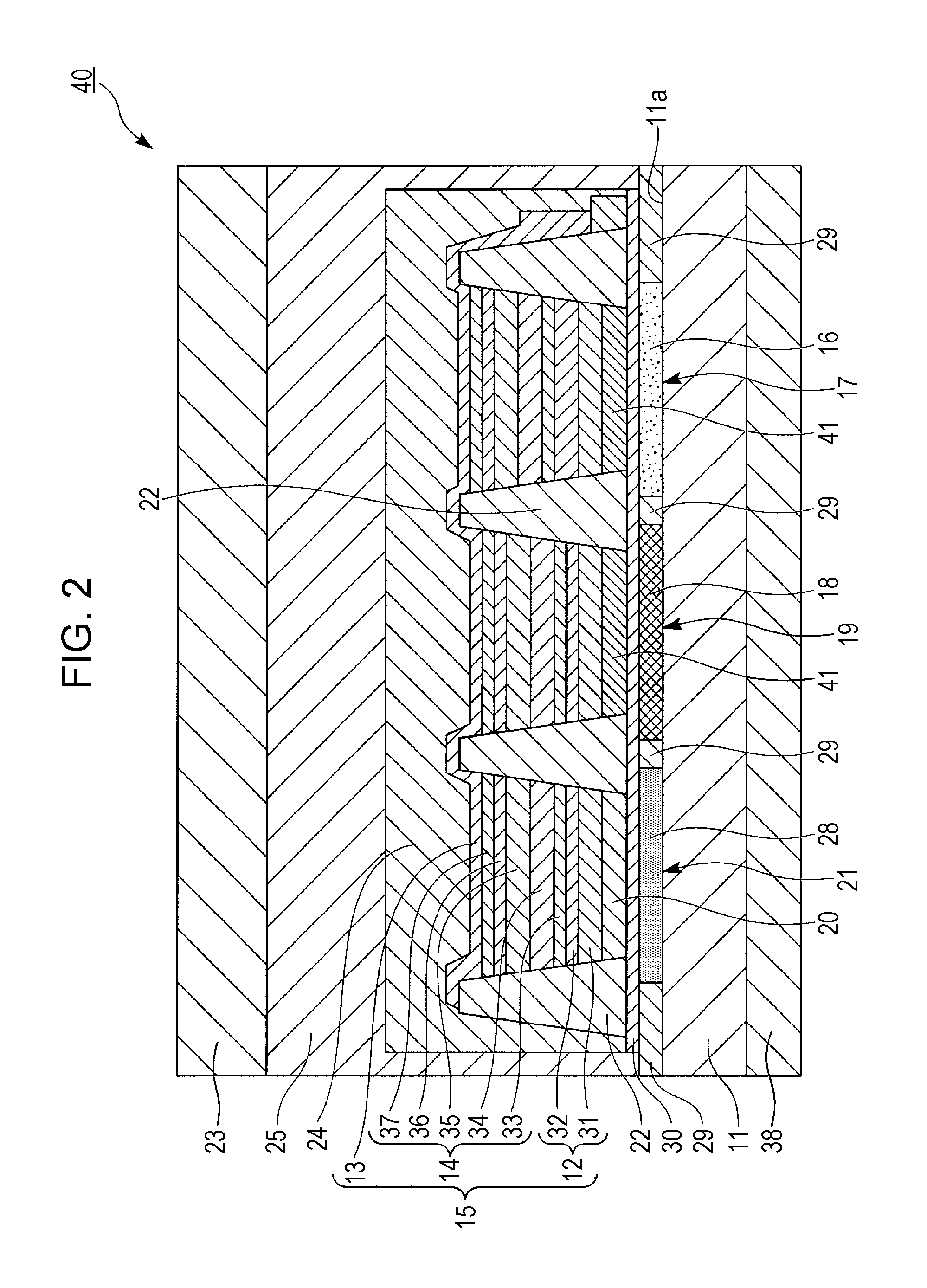
[0245]FIG. 2 is a schematic cross-sectional view of an organic EL display device according to a second embodiment. In FIG. 2, the same elements as those in the organic EL display device 10 illustrated in FIG. 1 are designated using the same reference numerals, and descriptions are not redundantly repeated.

[0246]An organic EL display device 40 according to this embodiment differs from the organic EL display device 10 according to the first embodiment in that a light-scattering layer 41 is disposed in the blue pixel portion 17 in place of the wavelength conversion layer 26 and that another light-scattering layer 41 is disposed in the green pixel portion 19 in place of the wavelength conversion layer 27.

[0247]The organic EL display device 40 includes pixel portions having different light distributions: the blue pixel portion 17 and the green pixel portion 19 that directly use anisotropic light emitted from the organic EL section 15 having a microcavity structure; a...

third embodiment

(3) Third Embodiment

[0255]FIG. 3 is a schematic cross-sectional view of an organic EL display device according to a third embodiment. In FIG. 3, the same elements as those in the organic EL display device 10 illustrated in FIG. 1 and the organic EL display device 40 illustrated in FIG. 2 are designated using the same reference numerals, and descriptions are not redundantly repeated.

[0256]An organic EL display device 50 includes the first substrate 11; the organic EL section 15 disposed on the first surface 11a of the first substrate 11, the organic EL section 15 including the organic layer 14 held between the first electrode 12 and the second electrode 13; the second substrate 23 disposed opposite the first substrate 11 with the adhesive layer 25; the blue pixel portion 17 including the blue color filter 16, the green pixel portion 19 including the green color filter 18, and the red pixel portion 21 including the wavelength conversion layer 20 that contains a wavelength conversion m...


PUM


Abstract

An organic EL display device includes an organic EL section including an organic layer held between a first electrode and a second electrode, one of the two electrodes serving as a reflective electrode, and the other serving as a translucent electrode; a blue pixel portion including a blue color filter configured to mainly transmit a light component in a blue wavelength region of light emitted from the organic EL section; a green pixel portion including a green color filter configured to mainly transmit a light component in a green wavelength region of the light emitted from the organic EL section; and a red pixel portion including a wavelength conversion layer configured to absorb at least one of the light component in the blue wavelength region and the light component in the green wavelength region of the light emitted from the organic EL section and emit light in a red wavelength region.

Description

TECHNICAL FIELD[0001]The present invention relates to an organic electroluminescent display device, an electronic apparatus including the same, and a method for producing an organic electroluminescent display device.[0002]This application claims the right of priority of Japanese Patent Application No. 2011-252735 filed Nov. 18, 2011, which is hereby incorporated by reference herein in its entirety.BACKGROUND ART[0003]Organic electroluminescent (hereinafter, also referred to as an “organic EL” or “organic LED”) displays have been attracting attention because they are self-luminous and a high-quality image is obtained. Unlike liquid crystal displays, the power consumption of organic EL displays is not increased by the fact that a trend toward higher definition causes lower aperture ratios. Thus, organic EL displays have been attracting attention in the field of smartphones and tablet terminals that are increasingly required to have further higher definition.[0004]To produce organic EL...

Claims


Application Information

Patent Timeline
Patent Type & Authority Applications(United States)
IPC IPC(8): H01L27/32
CPCH01L27/3211H01L27/322H10K59/35H10K59/38H10K59/12H10K59/879H10K50/858
Inventor FUJITA, YOSHIMASA
Owner SHARP KK
Why Eureka
Try Eureka