Multiport semiconductor memory device capable of sufficiently steadily holding data and providing a sufficient write margin

a memory device and multi-port technology, applied in the direction of information storage, static storage, digital storage, etc., can solve the problems of data being destroyed in the memory cell, difficult to write data, and difficult to ensure that data is held steady, so as to reduce current driving force ratio, sufficient write margin, and data holding significantly steady

Inactive Publication Date: 2007-01-09
RENESAS TECH CORP
View PDF4 Cites 22 Cited by
  • Summary
  • Abstract
  • Description
  • Claims
  • Application Information

AI Technical Summary

Benefits of technology

[0027]Thus the present multiport SRAM can prevent reduced current driving force ratios attributed to increased numbers of ports. The present multiport SRAM can hold data significantly steadily and provide a sufficient write margin.
[0028]Furthermore, each port can be used to read and write data, which can help to design.

Problems solved by technology

In other words, the data held in the memory cell is destroyed and as a result an erroneous operation is caused.
If the current driving force is set to high, however, the latch circuit enters an excessively stable state, which can render it difficult to write data.
Thus for multiport SRAMs it is increasingly difficult to ensure that data is held steadily and also ensure sufficient write margin.
Furthermore the above described, conventional multiport SRAM memory cell, in any configuration, has each port corresponding to only one of reading and writing data and does not allow a single port to accommodate both reading and writing data.
This is an obstacle to freely designing a circuit.

Method used


Image

  • Multiport semiconductor memory device capable of sufficiently steadily holding data and providing a sufficient write margin
  • Multiport semiconductor memory device capable of sufficiently steadily holding data and providing a sufficient write margin
  • Multiport semiconductor memory device capable of sufficiently steadily holding data and providing a sufficient write margin

Examples


first embodiment

[0045

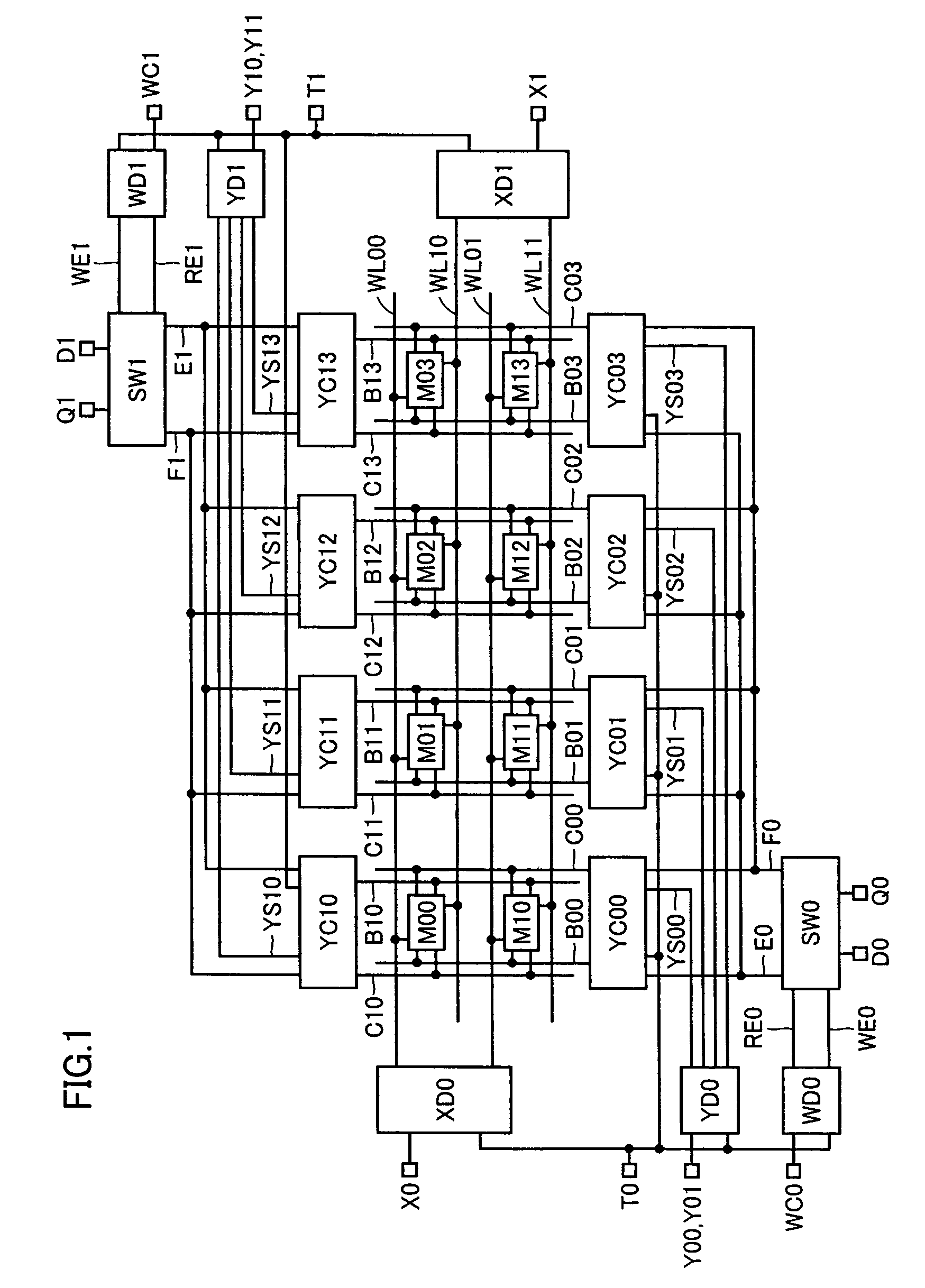
[0046]FIG. 1 is a schematic block diagram showing a configuration of a 2-port static semiconductor memory device of the present invention in a first embodiment.

[0047]While FIG. 1 shows a configuration of a 2-port SRAM having memory cells arranged in a matrix of two rows and four columns to simplify the description, the present invention is not limited to this configuration and is applicable to any multiport SRAMs having memory cells arranged in a matrix of more rows and columns.

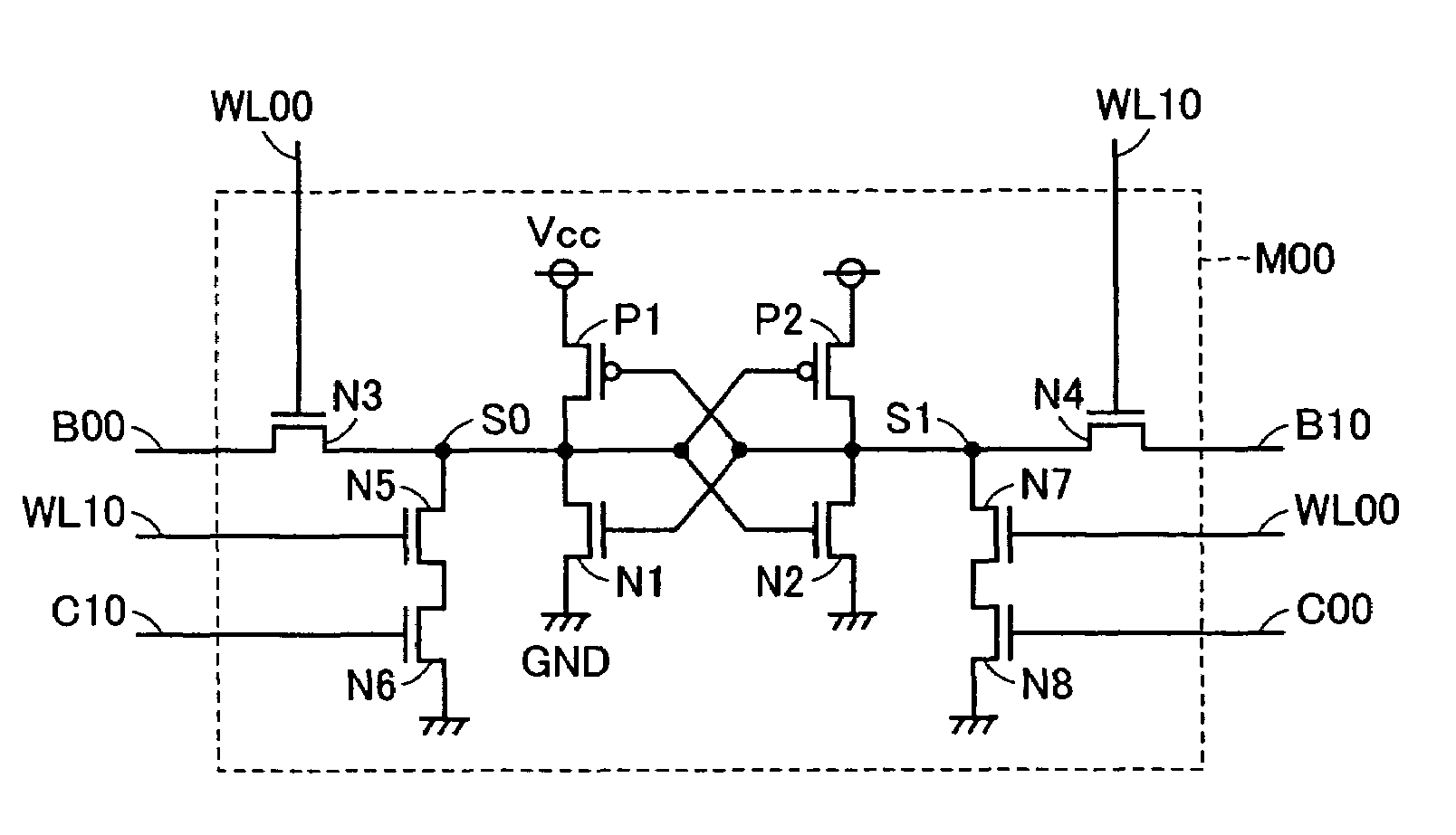
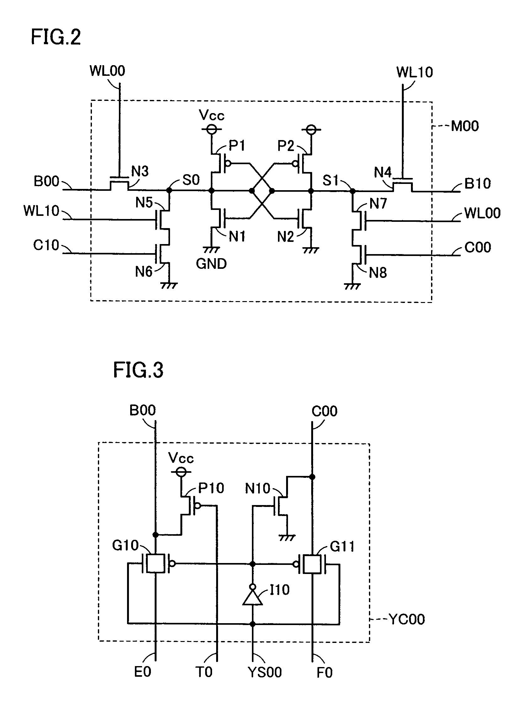
[0048]With reference to FIG. 1, the 2-port SRAM includes: a memory array having memory cells M00–M03, M10–M13 arranged in two rows and four columns; word lines WL00, WL10 associated with the row of memory cells M00–M03; word lines WL01, WL11 associated with the row of memory cells M10–M13; bit lines B00, B10 and sub bit lines C00, C10 shared by memory cells M00, M10; bit lines B01, B11 and sub bit lines C01, C11 shared by memory cells M01, M11; bit lines B02, B12 and sub bit lines C02, C12 shared by memo...

second embodiment

[0172

[0173]FIG. 10 is a schematic block diagram extracting and showing a configuration of a memory array of the present 2-port SRAM in a second embodiment.

[0174]With reference to the figure, the 2-port SRAM includes memory cells R[0]–R[k] arranged in k+1 rows and one column, word lines WL00, WL10 . . . WL0k, WL1k correspondingly associated with the rows of memory cells, bit lines B0 and B1 shared by memory cells R[0]–R[k], sub bit lines C0 and C1, and common signal lines Q0 and Q1 shared by memory cells R[0]–R[k], wherein k represents a natural number. Note that while in the present embodiment a single column of memory cells is used by way of example, a plurality of columns of memory cells may also be applicable.

[0175]Between common signal line Q0 and ground potential GND an n MOS transistor N41 is connected. Transistor N41 has a gate potential controlled via sub bit line C0.

[0176]Between common signal line Q1 and ground potential GND an n MOS transistor N40 is connected. Transistor...

third embodiment

[0196

[0197]FIG. 13 is a circuit diagram showing a configuration of the present multiport SRAM memory cell in a third embodiment.

[0198]With reference to the figure, the multiport SRAM memory cell, having 2n ports, wherein n is a natural number, includes a latch circuit formed of p and n MOS transistors P1 and N1 connected between power supply potential Vcc and ground potential GND in series and p and n MOS transistors P2 and N2 connected between power supply potential Vcc and ground potential GND in series.

[0199]MOS transistors P1, N1 have their respective gates both connected to a node S1 connecting MOS transistors P2 and N2. (Hereinafter this node will also be referred to as storage node S1.) MOS transistors P2, N2 have their respective gates both connected to a node connecting MOS transistors P1 and N1. (Hereinafter this node will also be referred to as a storage node S0.) In other words, p MOS transistors P1, P2 serve as load transistors and n MOS transistors N1, N2 serve as driv...


PUM


Abstract

A 2-port SRAM includes a memory cell having: a latch circuit holding potential at storage nodes complementarily; access transistors arranged between the storage nodes and bit lines, respectively, and turned on in response to word lines being activated; a write access transistor and a storage level drive transistor arranged between the storage nodes, respectively, and a ground potential and turned on in response to a first one of the word lines being activated and a sub bit line, respectively, and a write access transistor turned on in response to a second one of the word line being activated and a storage level drive transistor turned on in accordance with a sub bit line.

Description

BACKGROUND OF THE INVENTION[0001]1. Field of the Invention[0002]The present invention relates to semiconductor memory devices and particularly to configurations of multiport static random access memories (hereinafter referred to as multiport SRAMs).[0003]2. Description of the Background Art[0004]FIG. 14 is a circuit diagram of a configuration in a first example of a memory cell used for a conventional 2-port static random access memory (SRAM), as described for example in Japanese Patent Laying-Open No. 1-251384. This memory cell will hereinafter be referred to as a 2-port SRAM memory cell.[0005]As shown in FIG. 14, a 2-port SRAM memory cell M100 includes a latch circuit having p and n MOS transistors P100 and N100 connected in series between a power supply potential Vcc and a ground potential GND, and p and n MOS transistors P101 and N101 connected in series between power supply potential Vcc and ground potential GND.[0006]MOS transistors P100, N100 have their respective gates both ...

Claims


Application Information

Patent Timeline
Patent Type & Authority Patents(United States)
IPC IPC(8): G11C8/00G11C8/16G11C11/41G11C11/412G11C11/417G11C13/00
CPCG11C11/412G11C8/16
Inventor MORISHIMA, CHIKAYOSHI
Owner RENESAS TECH CORP
Why Eureka
Try Eureka