

Liquid crystal display device having an auxiliary electrode corresponding to the periphery of the pixel electrode in only one of at least two domain
- Summary
- Abstract
- Description
- Claims
- Application Information
AI Technical Summary
Benefits of technology
Problems solved by technology
Method used
Image

Examples
first embodiment
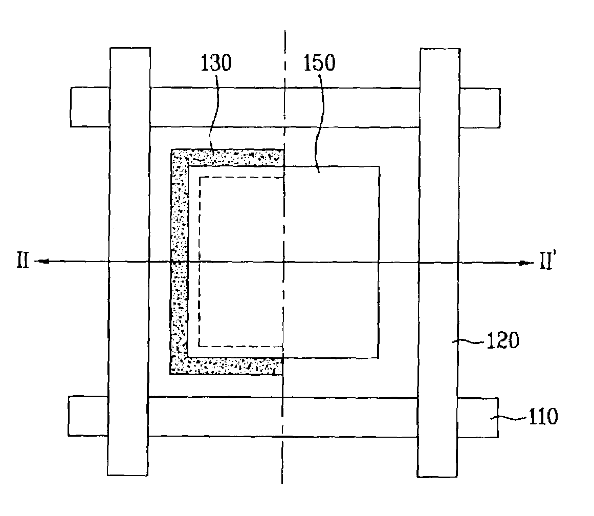
[0038]FIG. 2A is a plan view illustrating a pixel of an LCD device according to the present invention. FIG. 2B is a cross-sectional view illustrating an LCD device taken along line II–II′ of FIG. 2A when a voltage is applied.
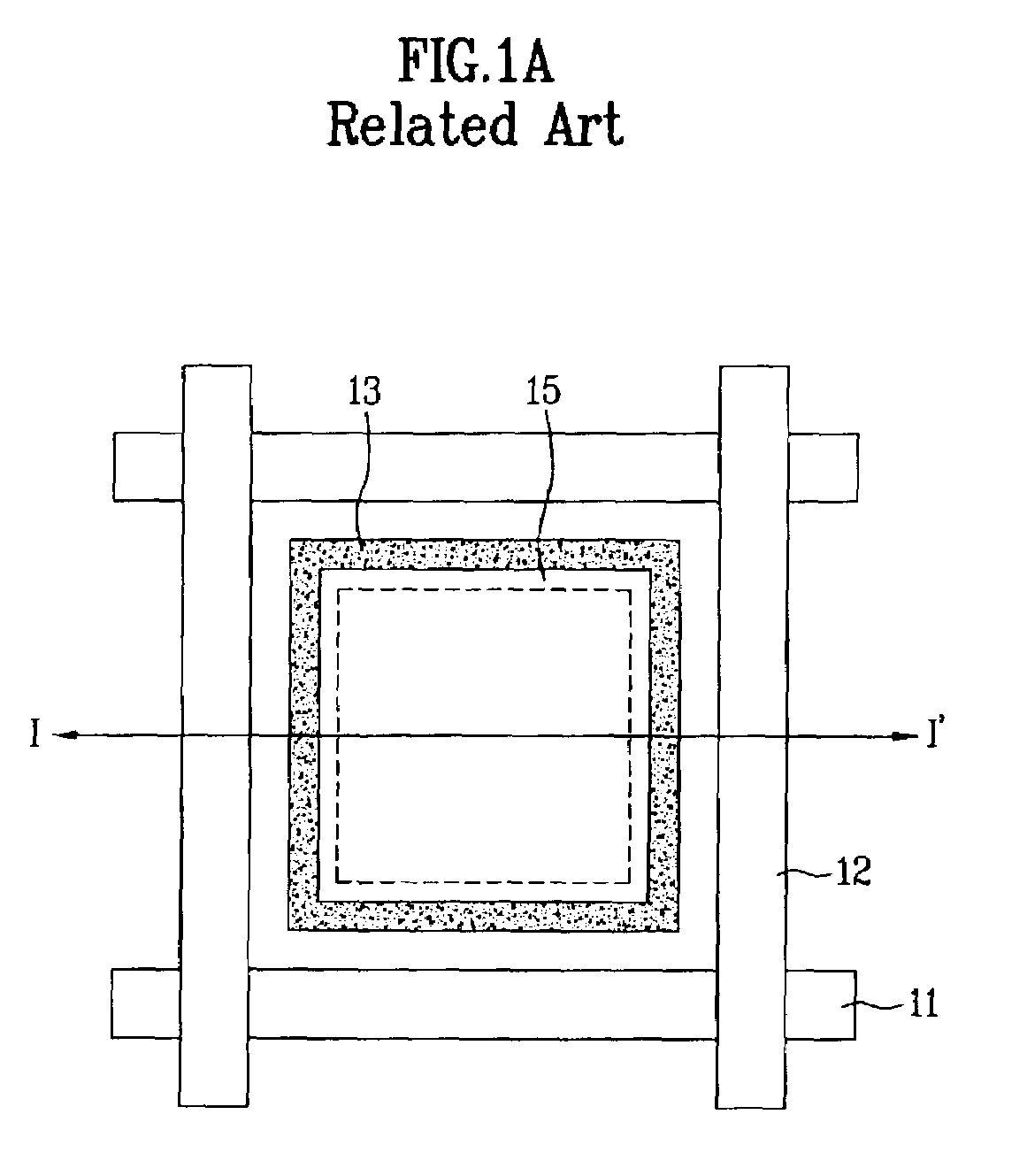
[0039]Referring to FIG. 2A, the LCD device according to the first embodiment of the present invention includes a plurality of gate lines 110 and data lines 120 crossing to each other for defining a plurality of pixel regions on a lower substrate 100, and a pixel electrode 150 in each pixel region. Also, an auxiliary electrode 130 is formed on the same layer as the data line 120, which is partially overlapped with the pixel electrode in the periphery of one region (domain) of the pixel region equally divided into two. That is, the auxiliary electrode is formed along the periphery of roughly half of the pixel electrode 150.
[0040]The structure of the pixel region and the lower and upper substrates will be explained in detail.
[0041]As shown in FIG. 2B, the lower sub...
second embodiment
[0053]FIG. 3A is a plan view illustrating a pixel of an LCD device according to the present invention, and FIG. 3B is a cross-sectional view illustrating an LCD device taken along line III–III′ of FIG. 3A when a voltage is applied.
[0054]In the LCD device according to the first embodiment of the present invention, the electric field is distorted to the outside direction of the pixel when dividing the domains of the pixel. Referring to FIG. 3A and FIG. 3B, the LCD device according to the second embodiment of the present invention is different from the LCD device according to the first embodiment of the present invention in that the electric field is distorted to the center direction of the pixel. For this, an electric field inducing window 160 is formed in a pixel electrode 150a, and an auxiliary electrode 130 is formed below the pixel electrode 150a to correspond to the electric field inducing window 160. A dielectric structure 260 is formed on a common electrode 240 corresponding to...
third embodiment
[0073]FIG. 4 is a cross-sectional view illustrating an LCD device taken along line III–III′ of FIG. 3A according to the present invention.
[0074]Referring to FIG. 4, the LCD device according to the third embodiment of the present invention is different from the LCD device according to the second embodiment of the present invention in that the electric field inducing window 160 is formed in the common electrode 240, the auxiliary electrode 130 is formed below the electrode 150a to correspond to the electric field inducing window 160, and the dielectric structure 260 is formed at a portion of the lower substrate 100 corresponding to the periphery of one domain (or to the periphery of the pixel electrode 150a in one domain) where the alignment direction of the liquid crystal molecules is different from the alignment direction of the first alignment layer. Except the aforementioned constituent elements, others are same as those of the LCD device according to the second embodiment of the ...
PUM
 Abstract
Description
Claims
Application Information