This helps you quickly interpret patents by identifying the three key elements:
Problems solved by technology
Method used
Benefits of technology
Benefits of technology
The present invention provides a liquid crystal display device with high aperture ratio, which allows for a clearer image to be displayed. However, this may require an increase in power consumption to compensate for the decreased aperture ratio. Overall, the invention aims to provide a high-quality, low-power, and highly reliable liquid crystal display device with high resolution.
Problems solved by technology
Thus, in a transmissive liquid crystal element or the like, the light intensity of a backlight needs to be increased to display a clear image, and power consumption is increased.
In addition, when pixel area is significantly decreased, it becomes difficult to design a horizontal electric field-mode liquid crystal element where a comb-shape electrode is positioned in a horizontal direction.
Thus, it also becomes difficult to increase a manufacturing yield.
Method used
Image
Click on the blue label to locate the original text in one second.
Reading with bidirectional positioning of images and text.
Examples
embodiment 1
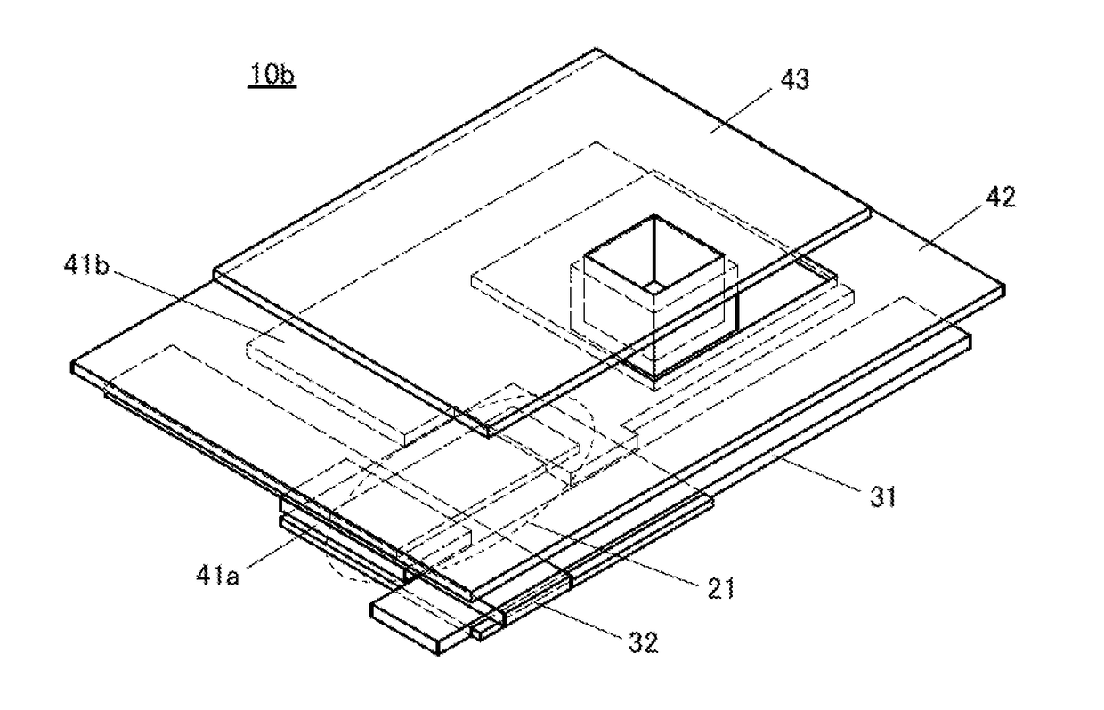
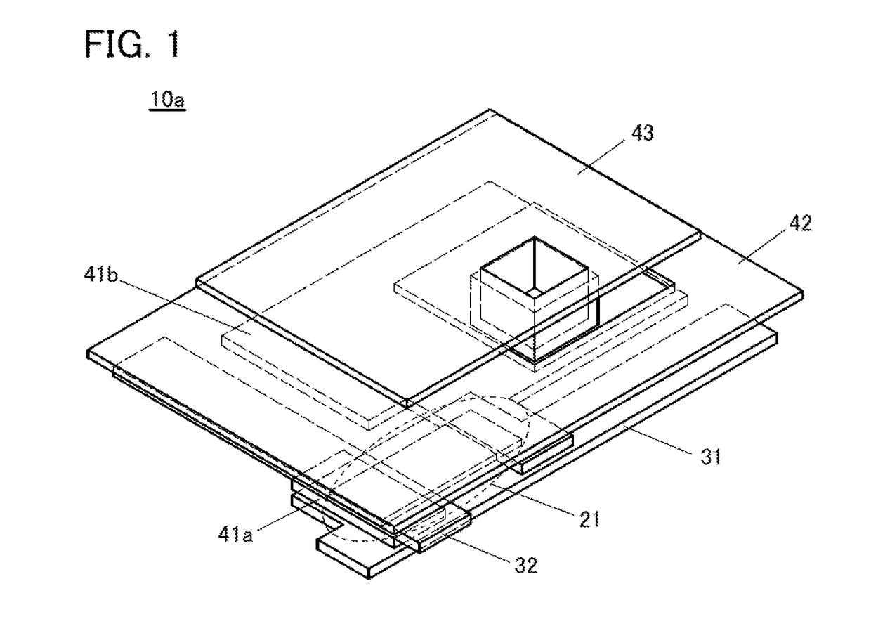
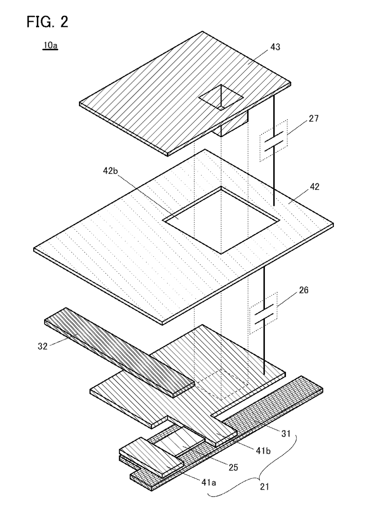
[0049]In this embodiment, a display device in one embodiment of the present invention is described.
[0050]The display device in one embodiment of the present invention includes a first conductive layer, a second conductive layer, and a liquid crystal element. In the liquid crystal element, a liquid crystal layer is positioned between a third conductive layer and a fourth conductive layer.
[0051]The first to fourth conductive layers transmit visible light and include a region where the first to fourth conductive layers overlap with each other. The second conductive layer is positioned between the first conductive layer and the third conductive layer.
[0052]An insulating layer is positioned between the first conductive layer and the second conductive layer. An insulating layer is positioned between the second conductive layer and the third conductive layer. Therefore, two capacitors each including the second conductive layer as an electrode are stacked.
[0053]The two capacitors transmit l...
embodiment 2
[0184]In this embodiment, an operation mode that can be employed in the display device in one embodiment of the present invention is described with reference to FIGS. 19A to 19C.
[0185]A normal driving mode with normal frame frequency (typically, higher than or equal to 60 Hz and lower than or equal to 240 Hz) and an idling stop (IDS) driving mode with low frame frequency are described below.
[0186]Note that the IDS driving mode refers to a method in which after image data is written, rewriting of image data is stopped. This increases the interval between writing of image data and subsequent writing of image data, so that power that would be consumed by writing of image data in that interval can be reduced. The IDS driving mode can be performed at frame frequency that is 1 / 100 to 1 / 10 of the normal driving mode, for example. A still image is displayed by the same video signals in consecutive frames. Thus, the IDS driving mode is particularly effective when displaying a still image. Wh...
embodiment 3
[0195]A metaloxide that can be used for a semiconductor layer of a transistor disclosed in one embodiment of the present invention is described in this embodiment. Note that when a metal oxide is used for a semiconductor layer of a transistor, the metal oxide may be referred to as an oxide semiconductor.
[0196]An oxide semiconductor is classified into a single crystaloxide semiconductor and a non-single-crystal oxide semiconductor. Examples of a non-single-crystal oxide semiconductor include a c-axis aligned crystalline oxide semiconductor (CAAC-OS), a polycrystalline oxide semiconductor, a nanocrystalline oxide semiconductor (nc-OS), an amorphous-like oxide semiconductor (a-like OS), and an amorphous oxide semiconductor.
[0197]A cloud-aligned composite oxide semiconductor (CAC-OS) may be used for the semiconductor layer of the transistor disclosed in one embodiment of the present invention.
[0198]Note that the non-single-crystal oxide semiconductor or the CAC-OS can be suitably used...
PUM
Abstract
A liquid crystaldisplay device with high aperture ratio is provided. The liquid crystaldisplay device includes a first conductive layer, a second conductive layer, and a liquid crystal element where a liquid crystal layer is positioned between a third conductive layer and a fourth conductive layer. The first to fourth conductive layers transmit visible light and include a region where the first to fourth conductive layers overlap with each other. The second conductive layer is positioned between the first conductive layer and the third conductive layer. An insulating layer is positioned between the first conductive layer and the second conductive layer. An insulating layer is positioned between the second conductive layer and the third conductive layer. Therefore, two capacitors each including the second conductive layer as an electrode are stacked. The two capacitors transmit light and overlap with the liquid crystal element; thus, aperture ratio can be increased.
Description
BACKGROUND OF THE INVENTION1. Field of the Invention[0001]One embodiment of the present invention relates to a liquid crystal display device and an electronic device.[0002]Note that one embodiment of the present invention is not limited to the above technical field. Examples of the technical field of one embodiment of the present invention include a semiconductor device, a display device, a light-emitting device, a power storage device, a storage device, an electronic device, a lighting device, an input device (e.g., a touch sensor), an input / output device (e.g., a touch panel), a method for driving any of them, and a method for manufacturing any of them.2. Description of the Related Art[0003]In recent years, attention has been drawn to a technique in which, instead of a siliconsemiconductor, a metaloxide exhibiting semiconductor characteristics is used for transistors. For example, Patent Documents 1 and 2 disclose techniques in which a transistor is manufactured using zincoxide...
Claims
Application Information
Patent Timeline
Application Date:The date an application was filed.
Publication Date:The date a patent or application was officially published.
First Publication Date:The earliest publication date of a patent with the same application number.
Issue Date:Publication date of the patent grant document.
PCT Entry Date:The Entry date of PCT National Phase.
Estimated Expiry Date:The statutory expiry date of a patent right according to the Patent Law, and it is the longest term of protection that the patent right can achieve without the termination of the patent right due to other reasons(Term extension factor has been taken into account ).
Invalid Date:Actual expiry date is based on effective date or publication date of legal transaction data of invalid patent.

